


Image from iStock
As chips have grown more powerful and transistor counts have soared into billions, IC substrates have evolved into a sophisticated multilayer structure that rivals the complexity of the chip itself.
This semiconductor component performs several essential functions simultaneously. It redistributes the dense array of microscopic connections on a chip’s surface to the wider pitch required for soldering onto a PCB. It channels power to the die and carry high-speed signals away from it while managing the thermal energy that modern processors generate. The IC substrate also provides mechanical support, protecting the delicate silicon from physical stress during assembly and throughout the device’s operational life.
The technology has undergone transformation over the past two decades. Early packages relied on lead frames and simple organic laminates, but today’s advanced substrates employ build-up layers with laser-drilled microvias, embedded components and line widths that approach those found on PCBs from decades ago. This evolution has been driven by demand from applications ranging from smartphones and data centers to artificial intelligence accelerators, where substrate performance increasingly determines overall system capability.
Types of IC substrates
IC substrates can be categorized based on their base material, manufacturing process and intended application.
Organic substrates represent the most widely used category in contemporary semiconductor packaging. These are constructed from layers of resin-impregnated fiberglass or other polymer-based materials, similar in concept to conventional PCBs but manufactured to far tighter tolerances.
BT resin has long been a workhorse material for organic substrates due to its favorable balance of thermal stability, electrical properties and cost. ABF has become the material of choice for high-performance applications, enabling the fine line widths and microvias required by advanced processors and graphics chips.
Organic substrates are lower cost and easier to process compared to ceramic alternatives, but face challenges with thermal expansion mismatch when bonded to silicon.
Ceramic substrates provide superior thermal conductivity and a coefficient of thermal expansion that more closely matches silicon, making them attractive for high-reliability and high-power applications.
Alumina ceramics have been used for decades in packages requiring hermetic sealing or operation in harsh environments. Aluminum nitride offers better thermal performance and finds use in power electronics and RF applications where heat dissipation is paramount.
LTCCs allow passive components such as capacitors and inductors to be embedded directly within the substrate, enabling compact RF modules and sensor packages. HTCCs, meanwhile, can withstand extreme operating conditions but require specialized processing.
The primary drawbacks of ceramic substrates, however, are their higher cost and the difficulty of achieving the fine features that organic substrates can provide.
Lead frame substrates use stamped or etched metal frames to provide both electrical connections and structural support. Copper alloys dominate this category due to their excellent electrical and thermal conductivity combined with reasonable cost.
Lead frames remain prevalent in discrete semiconductors, power management ICs and cost-sensitive consumer applications where the package complexity is modest. The technology now features exposed die pads for improved thermal dissipation and half-etched leads for finer pitch connections.
Silicon substrates and glass substrates have emerged as important options for advanced packaging schemes. Silicon interposers enable extremely fine redistribution layers and through-silicon vias, serving as an intermediate layer between chiplets in 2.5D packaging architectures. Glass substrates offer a combination of dimensional stability, low dielectric loss at high frequencies and the potential for large panel processing, positioning them as a promising technology for next-generation packages.
Embedded die substrates incorporate the silicon chip directly within the substrate layers rather than mounting it on top, enabling thinner packages and shorter interconnect lengths. This approach has gained traction in mobile devices and wearables where space is at a premium.
Many modern packages combine elements from multiple categories, such as organic substrates with embedded silicon bridges, reflecting the ongoing convergence of technologies in advanced semiconductor packaging.
China going for the high end
In China, the boom in 5G communication, artificial intelligence, Internet of Things and vehicle electrification is pushing manufacturers to accelerate R&D efforts. The goal is to reduce dependence on foreign technology and snare a share of the global market for advanced IC substrates, particularly those required for high-performance computing.
While this category remains dominated by Japan and South Korea, Chinese companies are working on minimizing line width and spacing, increasing layer count and realizing higher levels of electrical performance and thermal dissipation.
Such initiatives have yielded breakthroughs in recent years thanks to government support, including the inclusion of substrate technology in development plans. Companies such as Shennan Circuits, Shenzhen Fastprint and Kinwong turn out substrates for memory packages, midrange mobile applications and consumer electronics. These suppliers, which have invested heavily in expanding capacity and improving yields, are getting traction in the global market for standard BT-based substrates and simpler flip-chip packages. Shennan Circuits has an $830-million factory in Guangzhou and a $280-million facility in Wuxi, while Jiangxi Redboard has developed a technique in producing high-end IC substrates.
Chinese manufacturers are looking to expand their capabilities for ABF substrates as well as on prepeg-type build-up variants. The ABF category, used in advanced CPUs, GPUs, AI accelerators and high-bandwidth memory, remains dominated by industry giants such as Ibiden, Shinko Electric, Unimicron and Nan Ya PCB.
Coreless substrates are also on the agenda. Considered next-generation technology, they are superthin, which is said to be one-third to one-half of the thickness of conventional types because of the elimination of the core. In addition, they have a minimum line width and spacing below 10µm. For these attributes, these solutions have been adopted in FC-BGAs used in high-frequency and -density applications such as gaming and data centers. However, substrate strength and stability as well as production costs are still issues in this sphere, although improvements are expected in the coming years.
China’s mainstream selection
Widely manufactured IC substrates in China include flip-chip and wire bonding types. In terms of base materials used, there are rigid, flexible and ceramic options.
Rigid units form the bulk of shipments and consist mostly of ABF, BT and MIS kinds. ABF substrates are for high-performance CPUs and GPUs, while BT counterparts are mainly for MEMS and memory chips. MIS types are broadly used in power ICs and analog ICs. The typical specifications are four- to 20-layer count, 10µm line width and spacing, less than 1.5mm board thickness and less than 0.001 low dielectric loss.
TBD Electronics Co. Ltd, one of the suppliers interviewed by Global Sources, offers IC substrates with a complex multilayer buildup structure, low coefficient of thermal expansion and embedded thermal vias. These packages have a line width and spacing of less than 10µm and micro-, stacked and blind vias measuring 20 to 50µm.
Most resin substrate materials are imported. While there are Chinese suppliers, ABF materials are still largely sourced from Japan-based Ajinomoto, which accounts for over 90 percent or near monopoly of global supply. Copper-clad laminates, meanwhile, are widely available domestically, mainly from Kingboard, Shengyi, Nuoya and Wazam.
The rising cost of materials and demand for IC substrates will continue to keep product prices in an upward trend in the coming months.
Many Chinese manufacturers of IC substrates are found in Shenzhen, Dongguan, Zhuhai, Wuxi and Suzhou. Others are inland in Sichuan and Jiangxi provinces and in Chongqing. They are expected to drive the growth of China’s IC substrate market, the size of which is forecast to reach $8.81 billion in 2030 from $5.59 billion in 2023, according to Huajing Intelligence Network.
The products in this gallery have been handpicked by our China-based market analyst for representing current trends in IC substrates from Chinese makers.
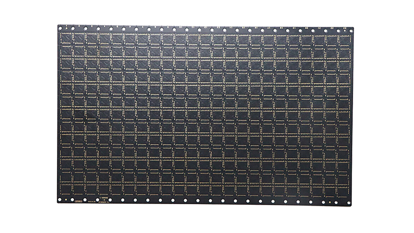
IC substrates made of FR-4, copper
Company: Dongguan Yuheng Hardware Products Co. Ltd
Available in custom sizes, the ICS-01 IC substrate from Dongguan Yuheng is based on an FR-4 base and copper materials.
MOQ: Negotiable
Lead time: 7 days
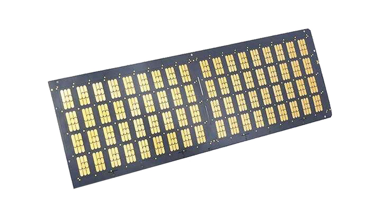
Control chip substrates, four-layer black core BT material
Company: Hong Kong Coben Hetron Technology Co. Ltd
The Control Chip Substrate from Hong Kong Coben uses a four-layer black core BT material with 0.33mm thickness and 75µm laser-drilled microvias.
MOQ: Negotiable
Lead time: 7 days
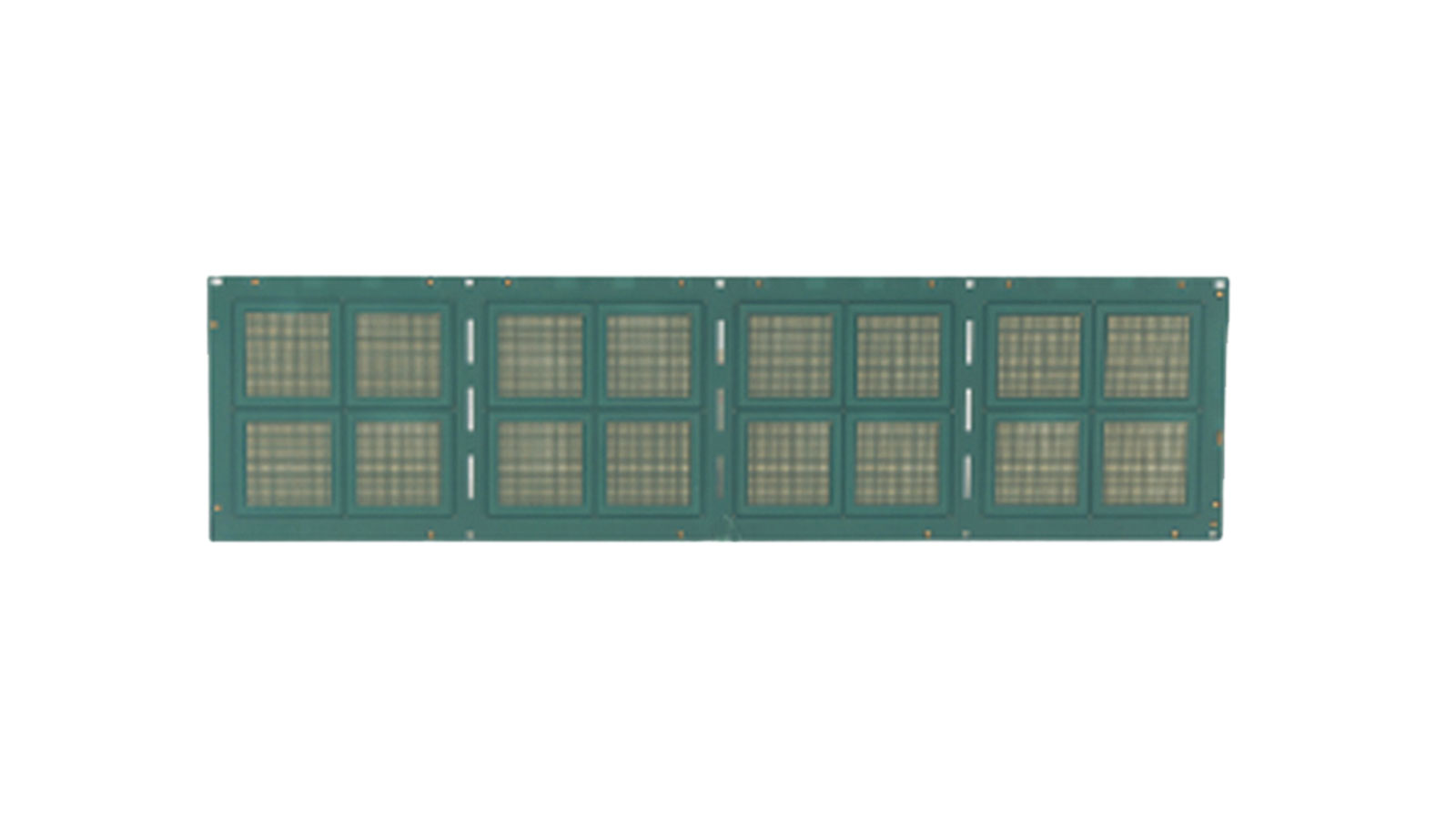
IC substrate with six-layer base
Company: Shenzhen Peak Technology Co. Ltd
Shenzhen Peak’s IC substrate, the SUB PCB-0001, is based on a six-layer board with 0.5mm finished thickness, 50µm minimum holes, 35µm minimum line width, 50µm minimum spacing, ENEPIG surface finish and green solder mask. The base material used is Shengyi Technology’s S1643HU.
MOQ: Negotiable
Lead time: 7 days
IC substrate with four to 20 layers
Company: TBD Electronics Co. Ltd
The 6073 from TBD is an IC substrate that comes in four- to 20-layer variants and has a low coefficient of thermal expansion. It has less than 10µm line width and spacing and 20 to 50µm blind or stacked microvias. Coreless and thin-core designs are available.
MOQ: Negotiable
Lead time: 7 days