Download App
Better Online and Trade Show Sourcing Experiences.Scan the QR code to download.
Learn More
Hot Topics
The chips have 8GB of memory and are 30 percent faster than 20nm DDR4 DRAM, which Samsung started producing in 2014.
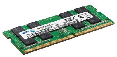
Samsung's 10nm DRAM supports a data transfer rate of 3,200Mbps (Source: EE Times)
Rumors about the death of Moore's Law have been greatly exaggerated in recent years, and Samsung Electronics' mass production of what the company said is the industry's first 10nm 8GB DDR4 DRAM chips shows DRAM scaling has yet to hit the proverbial wall.
In a news release, Samsung said its new DRAM supports a data transfer rate of 3,200Mbps, which is more than 30 percent faster than the 2,400Mbps rate of 20nm DDR4 DRAM. The new modules produced from the 10nm-class DRAM chips consume 10 to 20 percent less power compared to their 20nm process-based equivalents, making them ideal for high-performance computing systems, as well as the PC and mainstream server market.
Samsung said it addressed DRAM scaling challenges using currently available argon fluoride immersion lithography without the use of extreme UV equipment. The company began mass-producing 20nm 4GB DDR3 DRAM in 2014, and said its 10nm class DRAM is in part the result of its process a step further.
Samsung created the new 10nm cell structure by using a proprietary circuit design technology and quadruple patterning lithography, which enables use of existing photolithography equipment. Adoption of a refined dielectric layer deposition technology enabled further performance improvements, which engineers applied with uniformity to a thickness of a single-digit angstrom, which is one 10 billionth of a meter, on cell capacitors, resulting in sufficient capacitance for higher cell performance.
This article was originally published on EE Times. To read the rest of the article, please click here.
More Sourcing News
Read Also

关注 “环球资源外贸” 官方微信,获取实时外贸资讯
iOS & Android
iOS & Android(Mainland China)
Copyright © 2026 Publishers Representatives Limited. All rights reserved.