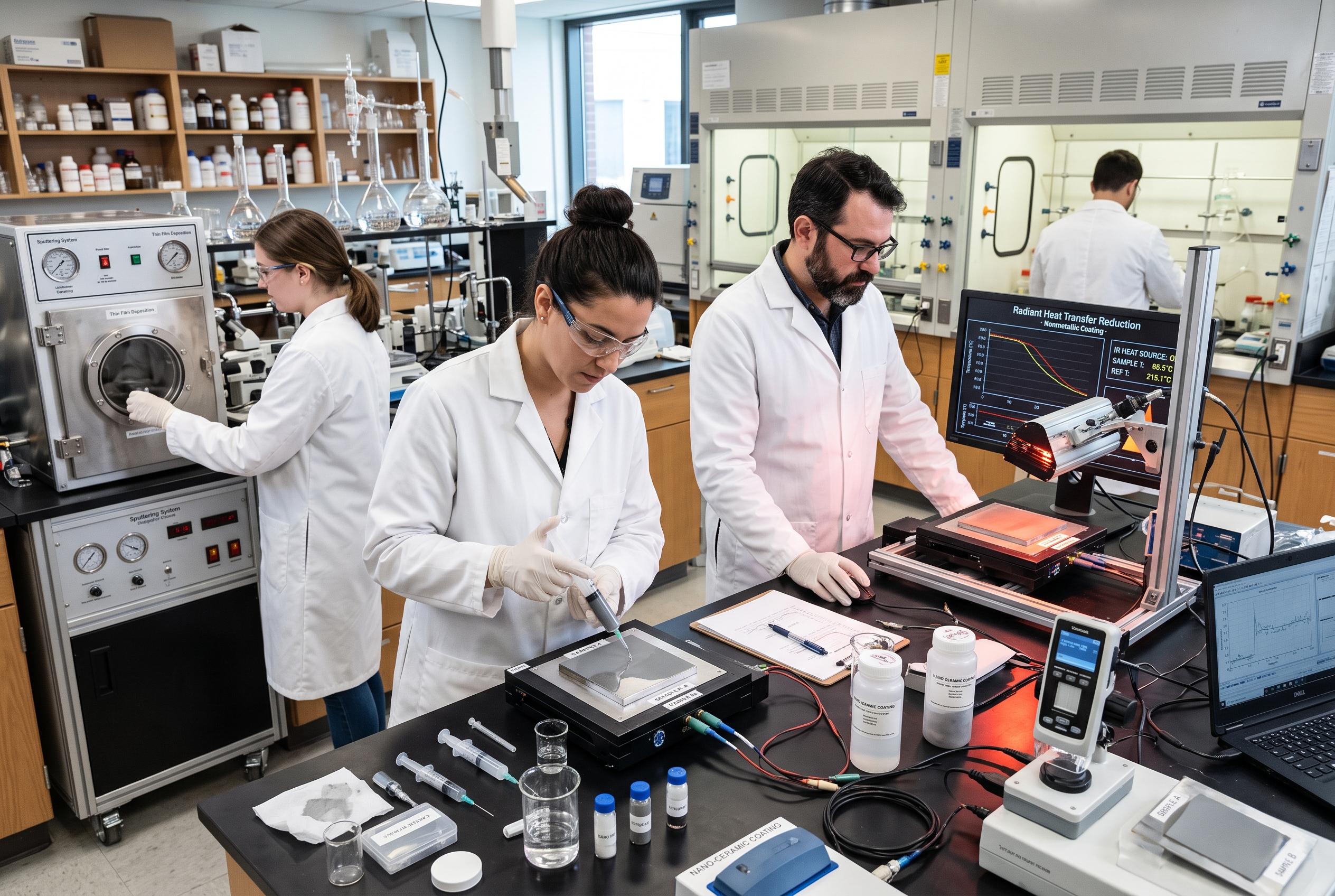
- Researchers develop a thin, nonmetallic coating that blocks radiant heat effectively
- Innovation uses coupled metasurfaces for broadband infrared control
- Potential applications in electronics, spacecraft and consumer devices with simplified manufacturing
Researchers at the CUNY Graduate Center’s Advanced Science Research Center, along with Honeywell Aerospace, have announced an interesting development: a thin, nonmetallic coating that, according to lab tests, can cut radiant heat transfer by more than 80 percent compared to common surfaces made from similar materials. This was published in Nature Communications, and it suggests a possible new way to approach thermal management in areas like electronics, spacecraft, infrared sensors and other systems where traditional metal coatings can cause electrical or integration issues.
Now, here’s where things get a little technical but worth understanding, heat does not always just spread through direct contact. At the temperatures we usually deal with, objects basically emit energy as invisible infrared radiation. That energy can hop between nearby surfaces even if they’re not touching. Metals often get used to block or reflect this infrared light because they are good at bouncing it back, but the problem is, they are also electrically conductive, which can be an issue in sensitive devices. Alternatives that are not metallic have been around, but many of those come with a trade-off, either they work with a narrow bandwidth or they need to be very thick, which is not always practical.
According to the researchers, their new approach involves treating two facing surfaces as a coupled system, so instead of trying for one surface to block everything by itself, both surfaces are designed to work together. Each of these "metasurfaces" is tuned to different parts of the infrared spectrum, so one side emits a lot where the other side absorbs less. The team likened it to radios set to different channels, this minimizes the amount of heat transfer between them.
The coatings were made up of seven ultrathin dielectric layers arranged as distributed Bragg reflectors. This kind of structure can selectively control how different wavelengths pass through it. And because the design does not rely on complicated nanoscale patterning, it can be manufactured using well-established thin-film fabrication techniques. That detail could be significant when it comes to scaling this up for industrial applications. The group also noted the coatings remained quite effective over a wide temperature range and were fairly tolerant of manufacturing inconsistencies.
For companies and professionals working in thermal management, the promise here is not just about how well they work but also about practicality. The whole concept is still at the proof-of-concept stage, so further testing will be needed before it hits the market. That said, the fact that it is based on existing materials and deposition methods used in thin-film production might help speed things along, making the leap from lab results to real-world use a bit less daunting.
What makes this especially interesting from an electronics and logistics perspective is that the innovation is not just about performance in a lab environment. In many real systems, the challenge is balancing thermal control with electrical isolation, weight, durability and compatibility with assembly processes. A coating that can be integrated without introducing conductive pathways could help engineers simplify designs in compact electronics, sensor housings and mobile devices where every layer matters. In the broader supply chain, that matters too: materials that use conventional thin-film sourcing and standard fabrication tools are often easier to evaluate for procurement, qualification, and manufacturing consistency.
The potential applications also stretch into lifestyle-facing technology, even if the users of those products never see the coating itself. Smartphones, wearables, portable medical tools and consumer sensing devices all rely on carefully managed heat flow. As electronics become thinner and more powerful, thermal bottlenecks can limit battery life, performance and comfort. A nonmetallic solution that handles radiant heat more efficiently could support slimmer enclosures, quieter passive cooling and fewer compromises between design and reliability. In that sense, the work connects advanced materials science to everyday product development.
It is also worth noting that the idea of pairing two surfaces as a coupled thermal system may influence how future coatings are engineered. Instead of focusing only on one side of a barrier, designers could think in terms of matched components that interact across a controlled infrared window. That approach could be useful in spacecraft, where weight savings are critical, but also in industrial equipment, labs, and optical systems where stray heat can affect measurement accuracy. If the concept continues to hold up in testing, it could become part of a larger toolkit for next-generation thermal management.
For now, the most important takeaway is that the research suggests a practical path forward. Many advanced materials perform well only under tightly controlled conditions, or they rely on fabrication methods that are hard to scale. Here, the combination of dielectric layers, thin-film compatibility and broadband performance makes the concept feel closer to deployment than many experimental coatings. That does not mean immediate adoption, but it does make the case that useful innovation in electronics and heat control may come from rethinking how surfaces work together rather than forcing one material to do everything alone.
Takeaways / FAQ
Q: What is the main breakthrough here? A: A thin nonmetallic coating that significantly reduces radiant heat transfer without relying on conductive metal layers.
Q: Why is that important for electronics? A: It could help manage heat while avoiding electrical interference, which is useful in sensitive and compact devices.
Q: Is this ready for commercial use? A: Not yet. It is still at the proof-of-concept stage and needs more testing.
Q: Why does the manufacturing approach matter? A: Because it uses established thin-film methods, which may improve sourcing, scalability, and logistics for future production.
Q: Where could it matter most? A: Electronics, spacecraft, infrared sensors, and other systems needing thermal control without metallic coatings.
Disclaimer: This article may have been created with AI assistance and reviewed by our editorial team. It is provided for general informational purposes only. Readers should verify information independently before relying on this content.
Source Reference Map
Inspired by the headline at: 1
Sources by paragraph: