




Images from iStock
Semiconductor materials are the foundation of modern electronics, from smartphones and computers to solar cells, communication systems and electric vehicles (EVs). They have special electrical properties that allow engineers to control the flow of current precisely, making them essential across electronics applications. Over time, semiconductor technology has evolved through several generations of materials.
Si and Ge
The first generation of semiconductor materials is represented mainly by silicon (Si) and germanium (Ge). These materials were the earliest to be widely studied and used in electronic devices.
Silicon is abundant, relatively inexpensive and thermally stable. It forms silicon dioxide, a high-quality natural oxide, which is extremely useful in manufacturing transistors and integrated circuits. Because of these advantages, this material is still the primary material used in microprocessors, memory chips and many power devices.
Germanium, meanwhile, has higher electron and hole mobility than silicon, allowing faster charge transport. However, it is more sensitive to temperature and generally less stable in high-temperature environments. As a result, its role declined in mainstream electronics, although it still finds use in specialized high-speed devices, infrared optics and certain advanced semiconductor structures.
GaAs and InP
The second generation includes compound semiconductors, especially gallium arsenide (GaAs) and indium phosphide (InP). These materials were developed to overcome some limitations of silicon in high-frequency and optoelectronic applications.
Gallium arsenide offers higher electron mobility than silicon, making it well suited for high-speed and high-frequency devices. It is widely used in microwave circuits, satellite communications, radar systems and light-emitting devices. GaAs is also a direct bandgap material, which means it can efficiently emit and absorb light, an advantage in lasers and solar cells.
Indium phosphide is especially important in fiber-optic communication systems. It performs very well at the wavelengths used in optical telecommunications and is commonly used in photodetectors, laser diodes and high-speed integrated circuits. InP is valued for its excellent electron velocity and strong performance in advanced photonic applications.
Although GaAs and InP provide superior speed and optical performance compared with silicon, they are generally more expensive and more complex to manufacture. For this reason, they are often used in specialized fields rather than mass-market electronics.
GaN and SiC
The latest major development in semiconductor materials is the rise of third-generation semiconductors, particularly gallium nitride (GaN) and silicon carbide (SiC). These are called wide-bandgap semiconductors because they can operate at higher voltages, temperatures and frequencies than earlier materials.
Gallium nitride has attracted major attention for high-power and high-frequency applications. It can switch very quickly and operate efficiently in compact systems, making it ideal for modern power electronics, 5G base stations, fast chargers, RF amplifiers and aerospace systems. GaN devices are helping reduce energy loss while enabling smaller and lighter designs.
Silicon carbide has excellent thermal conductivity, high breakdown electric field strength and strong durability. These qualities make it especially valuable in high-voltage and high-temperature environments such as electric vehicles, renewable energy converters, industrial motor drives and smart power grids. SiC devices can improve energy efficiency and reduce cooling requirements, which is critical in demanding power systems.
China’s SiC substrate overtures
Research institutes, universities and enterprises in China have been pursuing the development of GaN and SiC materials with the goal of achieving industrialization. Some efforts have already yielded breakthroughs.
A first-tier SiC substrate material enterprise in the country, Shandong Tianyue Advanced Technology (SICC) introduced what it claims as the world’s first 12-inch SiC substrate at SEMICON China in March 2025. This was the result of innovations developed by researchers at Shandong University, including 12-inch SiC growing and laser lift-off technologies as well as equipment for 4H-SiC crystal growing and substrate processing.
In the same year, Tiancheng Semiconductor announced a breakthrough in 12-inch silicon carbide. Using its self-developed long crystal equipment, it was able to produce high-purity semi-insulating and N-type 12-inch SiC single crystals.
Industrialization underway
In 2025, China produced 4.2 million SiC substrates, 2.3 million epitaxials and 1.9 million wafers, and 960,000 GaN epitaxials and 740,000 wafers, according to the China Advanced Semiconductor Industry Innovation Alliance (CASA).
These figures, a core part of the country’s semiconductor bid, will continue to rise to secure domestic self-sufficiency. According to CASA, in the field of SiC substrates, localization will increase to 87 percent in 2027 from 80 percent in 2024.
Industrialization efforts are expected to accelerate and support this trend in the coming years.
In 2024, for instance, Beijing TanKeBlue and Shenzhen Major Industry Investment Group announced the opening of the Third-Generation Semiconductor SiC Material Industrial Park Project. This undertaking entailed a total investment of $467 million. It will turn out 100,000 6-inch SiC substrates and 250,000 epitaxials every year after entering mass production. These materials will cater to requirements mainly in automotive electronics, new energy, industrial control and consumer electronics. In addition, a new project for 8-inch SiC substrate and epitaxial research and industrialization is underway.
Zhejiang Jingsheng Mechanical & Electrical (JSG), meanwhile, has set up a subsidiary in Malaysia called SuperSiC, which broke ground on a 40,000sqm manufacturing facility in Seberang Perai in 2025, according to the Malaysian Investment Development Authority. Once running, phase 1 of the project will have an annual production capacity of 240,000 SiC wafers.
Fast-paced application
Globally, the market for GaN and SiC power devices is projected to reach $21.06 billion in 2031, with the latter type accounting for the majority share. This is a 21 percent CAGR from 2025, according to Market Monitor Global, thanks to automotive, industrial, telecom, infrastructure, consumer electronics and medical applications.
In 2030, the Yole Group said that automotive and mobility, industrial, and telecom and infrastructure will account for 70, 28 and 1 percent, respectively, for the SiC power device segment. In the GaN category, automotive and mobility, telecom and infrastructure, and energy will be the top demand drivers.
A similar trend in China is expected, according to CASA. In 2025, there was already a 28.6 percent year-on-year increase, with GaN and SiC power devices collectively reaching $3.24 billion.
China-made SiC and GaN materials
Silicon carbide materials available in China have a bandgap of 2.99 to 42.6eV for normal operation in temperatures as high as 600 C and a saturation electronic drift speed of 2x107cm/s or twice as fast as silicon counterparts.
GaN materials have a direct bandgap of 3.4eV and a thermal conductivity of 1.3W/cm-K, ensuring devices operate normally above 175 C.
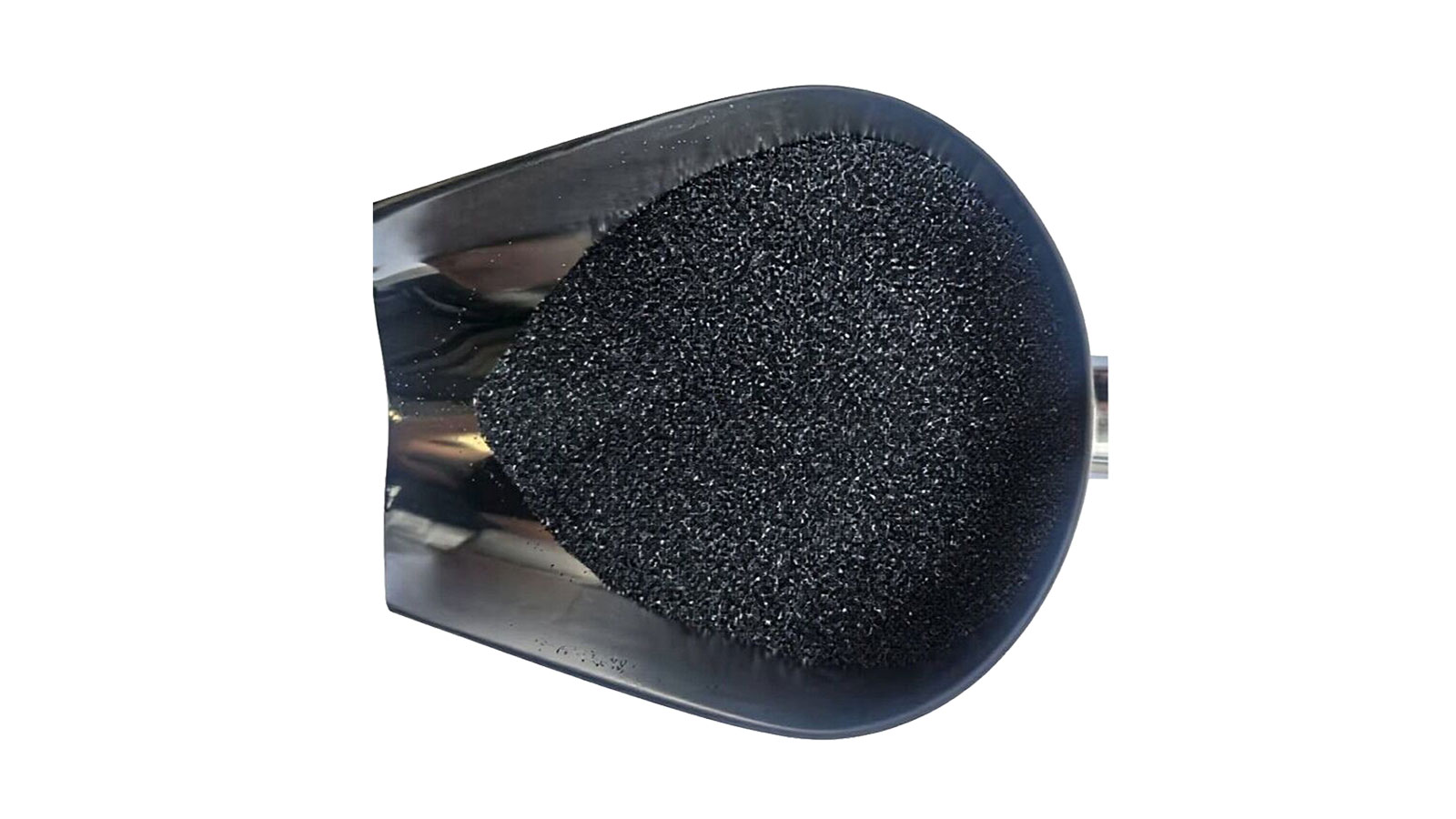
Quanzhou Huangbo Group Co. Ltd offers the HB-H-610, a nano SiC powder with 99 percent purity, ultrahigh hardness, and enhanced chemical, corrosion and temperature resistance as well as long functional life span. The MOQ can be negotiated and the lead time is seven days.
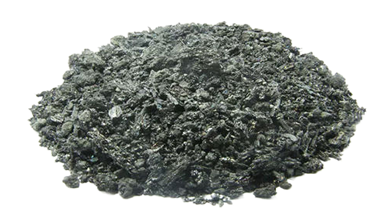
The SiC material from Xiamen Yuxiang Magnetic Materials Technology Co. Ltd is available in grain sizes of 0 to 5 or 10mm and 1 to 10mm. A minimum order of 1 ton is required and is shipped in seven days.
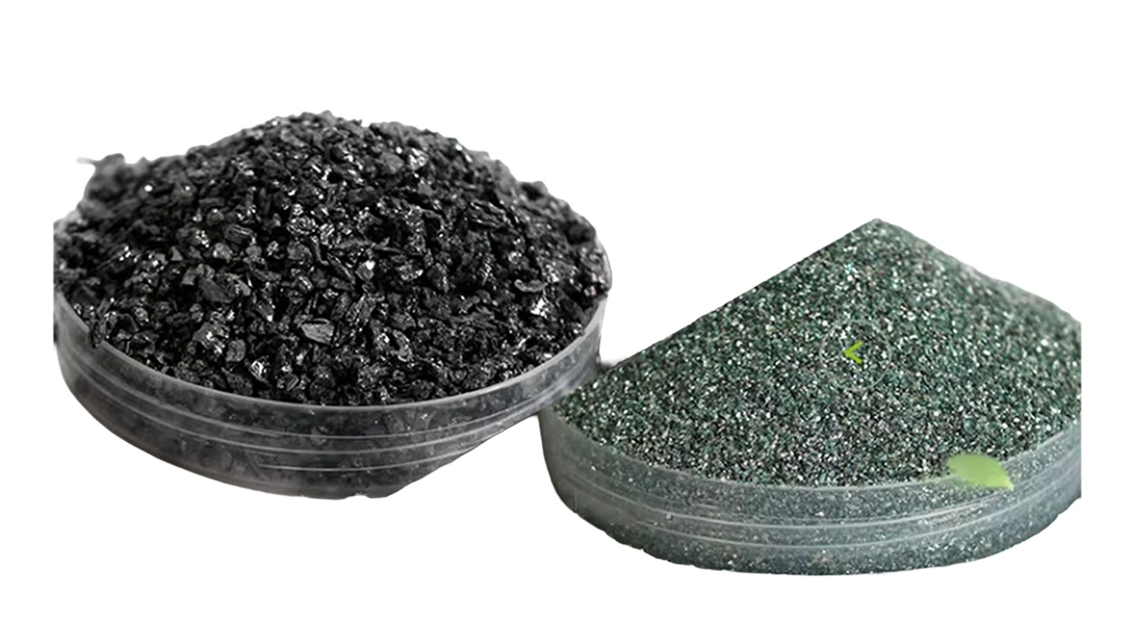
Zhengzhou Rongsheng Refractory Co. Ltd’s RS SiliconCarbide #9 has small thermal expansion and high thermal conductivity and corrosion resistance. The refractory grade is available in 0 to 1mm, 1 to 3mm, 3 to 5mm and 5 to 8mm, while the abrasive kind is in 12, 14, 16, 20, 24, 30, 36, 40, 60, 80, 100, 120, 150, 180, 200, 240, 280 and 300 mesh. The MOQ is 1 metric ton and the lead time is seven days.
Prices of SiC and GaN materials plummeted in 2025, but the spike in demand in mid-2026 resulted in increases. The cost of gallium doubled, leading to a sharp rise in quotes for GaN materials. It remains to be seen if input costs will stabilize in the coming months.
There are about a hundred suppliers of GaN and SiC materials in China, with SICC and TanKeBlue among the top three in the global SiC substrate segment and Epiworld and TYSiC in SiC epitaxials.