


As more smartphones, tablet PCs and other mobile electronics come in ever slimmer designs yet perform many functions, they need components that are ultracompact but enable powerful features.
In PCBs, HDI types are increasingly used in these devices as they meet all the miniaturization and performance requirements. In addition, there are advancements in this product category, adding advantages to its stack. In a report by Lucintel, these include a higher layer count that enhances these PCBs’ already complex routing feature further without impact on signal integrity, and advanced materials with better electrical and thermal management features.
Lucintel has forecast that the HDI PCB market will realize a 5 percent CAGR between 2023 and 2030 and reach $21 billion by the end of the period. This shows its expanding presence, especially in the consumer electronics, telecom, data communications and automotive industries. Prismark, meanwhile, has projected that HDI PCBs will beat the CAGR of the entire PCB market from 2023 to 2028. And some industry analysts venture as far as predicting that HDI PCBs will replace standard types in key market mobile electronics in the years ahead.
PCB manufacturing hub
China is the largest producer of PCBs. Its production value reached $37.794 billion, accounting for 54.4 percent of the global total in 2023, and will increase to $46.18 billion by 2028, according to Prismark. Based on statistics from AskCI, HDI PCBs had 18 percent share of China’s total PCB shipments in 2023 and more than half of the HDI board shipments were for mobile electronics devices.
There are about 200 manufacturers of HDI PCBs in the country and are found in Shenzhen, Dongguan, Zhongshan, Huizhou, Zhuhai, Suzhou, Kunshan, Changzhou, Nanjing, Ningbo, Chengdu, Xi’an and Dalian.
More than 70 percent of these companies are small and midsize enterprises that are domestically owned. The top homegrown players include Victory Giant, Avary, WUS, Shennan Circuits and Kinwong.
Avary, a first-tier global PCB supplier, specializes in the development and production of superthin HDI boards for high-end smartphones, tablet PCs and wearable devices. Its Huai’an factory in Jiangsu can output 93,000sqm every month.
For most Chinese makers, HDI PCBs account for 20 to 40 percent of shipments, a ratio that may get higher in the next several years thanks to healthy demand in the mobile electronics market. In China alone, this application base is expected to be in the scale of $527 billion by 2025, according to Beijing Boyan Zhishang Information Consulting.
This positive outlook, in turn, has been inviting investment. Fonder, a leading Chinese PCB supplier, set aside $95.83 million for the second phase of its high-layer HDI PCB project. The facility will start mass production in late 2024. Kinwong’s new factory, meanwhile, will be fully operational in 2025. The company targets to reach an annual output of 600,000sqm HDI PCBs.
Midrange and high-end HDI PCBs
In China, PCB manufacturers will continue to focus their R&D on midrange and high-range HDI types for mobile electronics applications. The areas for further improvement are the layer count, line width and spacing, and via diameter.
Companies such as Wonderful PCB (HK) Ltd can offer HDI PCBs with up to 28 layers, 3mil minimum line width and spacing and 0.0762mm minimum drilled hole size.
The widely available HDI PCBs for mobile devices, however, have a maximum layer count of eight and minimum sizes of 0.25mm for mechanical and 0.1mm for laser-drilled holes. The other specifications of typical products are 1 to 6oz copper, OSP, HASL, lead-free HASL, ENIG and immersion gold surface treatment options and 1.6mm board thickness. Most comply with industry safety standards such as UL, CE and RoHS.
These HDI PCBs are made using copper-clad laminates, copper foil and adhesive obtained domestically, with companies leveraging the advantage of being near the source of CCLs.
China is the world’s largest manufacturing hub for these laminates and is projected to turn out 1.09 billion square meters in 2024, according to AskCI. The top suppliers include Kingboard, Shengyi and Nan Ya.
Despite this proximity to CCL companies, most Chinese HDI PCB manufacturers were hit by a material cost increase and raised their prices in the past 12 months. They are optimistic that outlay for inputs will stabilize in the coming months and keep HDI PCB quotes from rising further.
Here are HDI PCBs that have been handpicked by our market analyst for representing current trends in China.
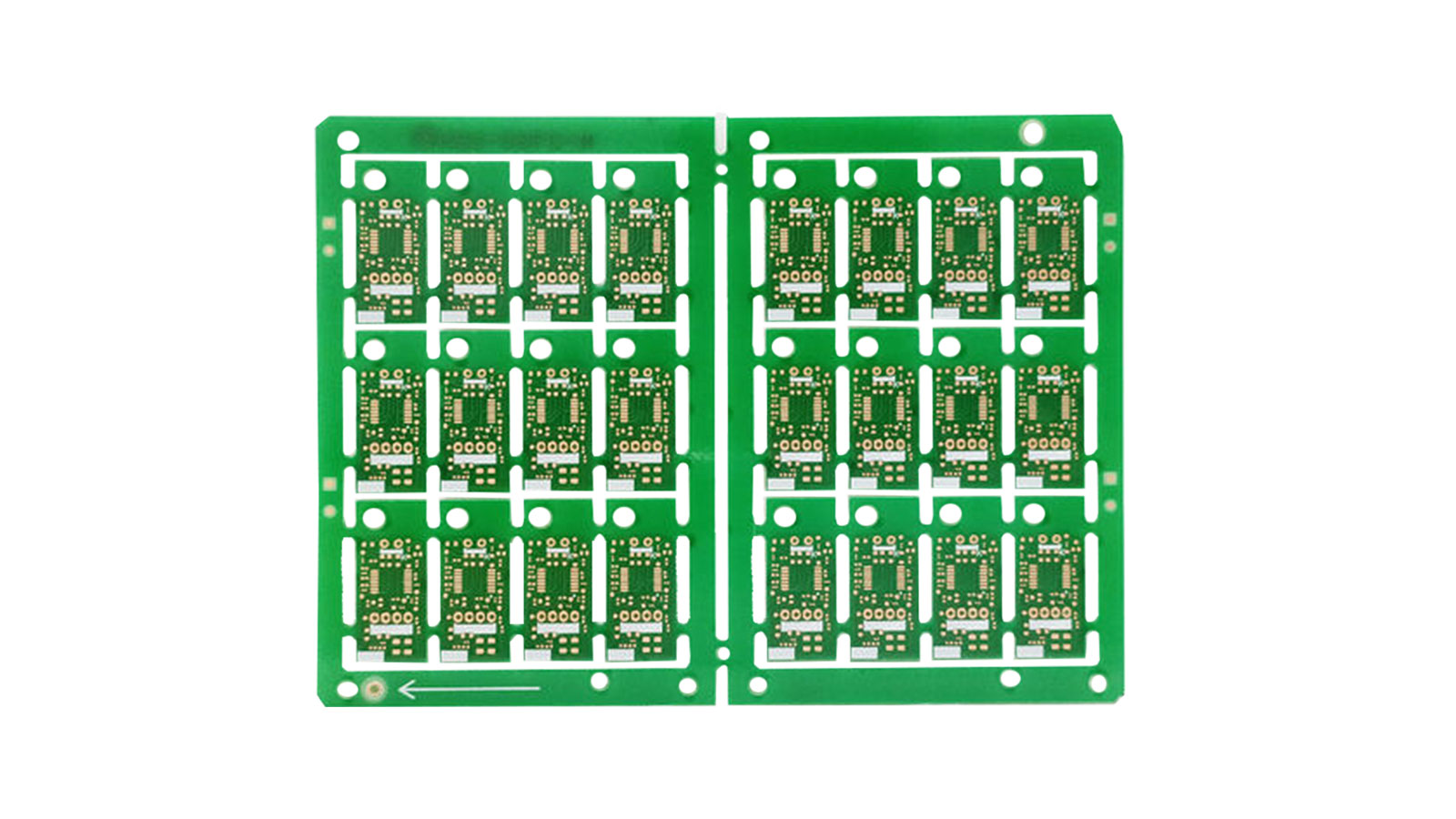
HDI PCB, 4mil minimum line width, spacing
Company: Dongguan Yuk Shing PCB Co. Ltd
With an immersion gold or lead-free HASL surface finish, the FR-4 P1 HDI PCB from Dongguan Yuk has as small as 0.2mm holes, 1 to 6oz copper thickness, and 4mil minimum line width and spacing.
MOQ: 1,000 units
Lead time: 15 days
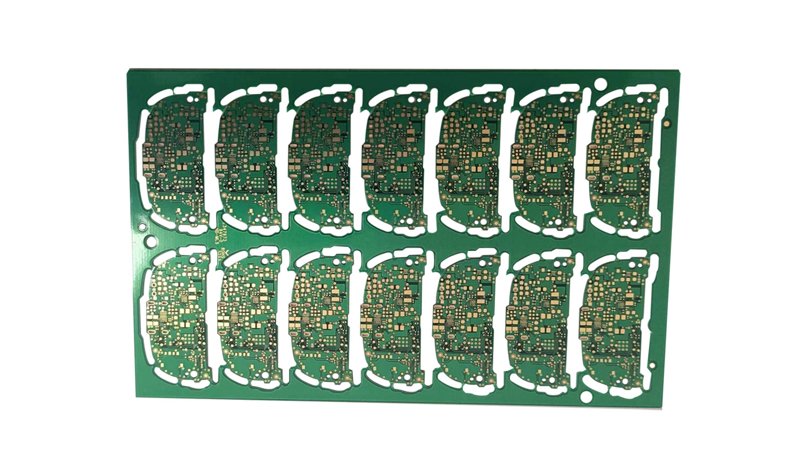
HDI PCB, up to 12 layers
Company: Huading Group Co. Ltd
Huading’s FR4-ENIG HDI PCB is available in up to 12-layer variants and has 5.9mil minimum line width and spacing, 0.2mm minimum hole size and an anti-oxidation surface finish.
MOQ: Negotiable
Lead time: 14 days
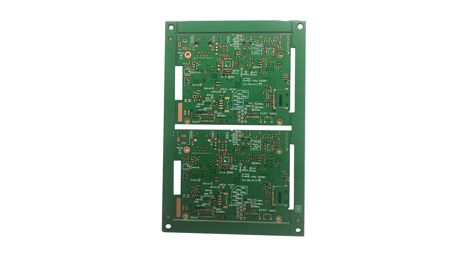
HDI PCB, eight layers
Company: Shenzhen GK Circuits Co. Ltd
The MS-2207-1226 from Shenzhen GK is an 8-layer HDI PCB with 0.25 and 0.1mm minimum mechanical- and laser-drilled holes, 2.99mil inner line width and 3.18mil spacing, 2.99mil outer line width and 3.8mil spacing, and OSP, ENIG or HASL surface finish. The board’s thickness is 1.6mm.
MOQ: Negotiable
Lead time: 5 days
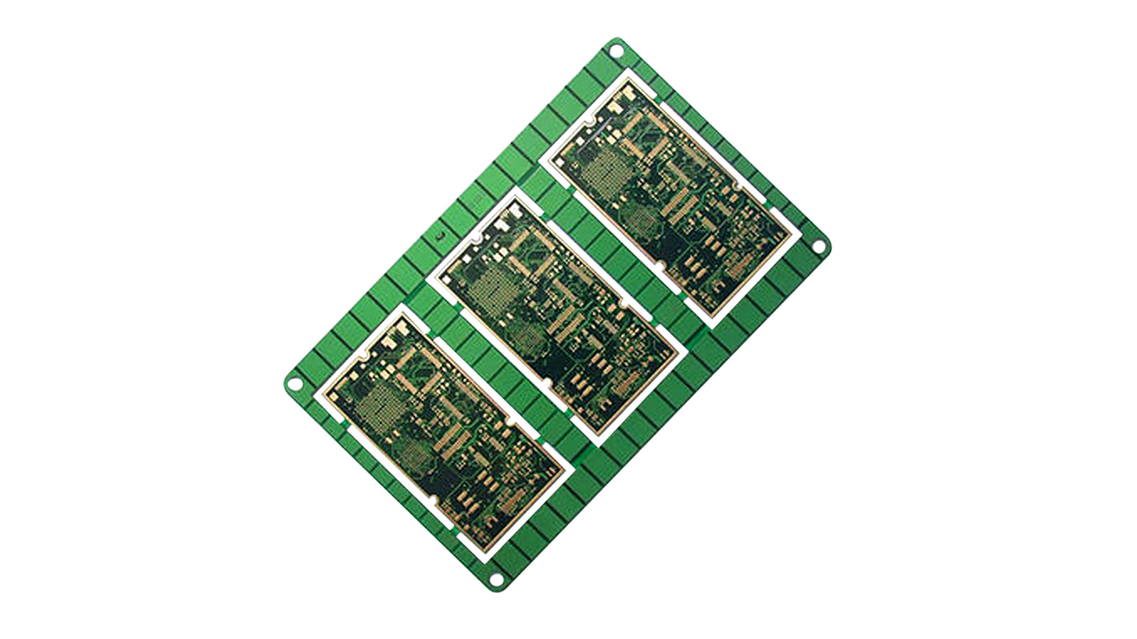
HDI PCB, up to 28 layers
Company: Wonderful PCB (HK) Ltd
With Rogers 4350 base material, this HDI PCB from Wonderful, the Wdf-07-23-7, has up to 28 layers, 3mil minimum line width and spacing, 0.0762mm minimum drilled hole size, 1oz copper, lead-free HASL, HASL, HAL, chemical tin or gold, immersion silver or gold, OSP or gold-plated surface finish and green, yellow, black, white, red or blue solder mask. The board thickness is 2.4mm.
MOQ: 1 unit
Lead time: 7 days