Download App
Better Online and Trade Show Sourcing Experiences.Scan the QR code to download.
Learn More
Hot Topics
NCSU tests low-cost PRESiCE process at TI's X-Fab.
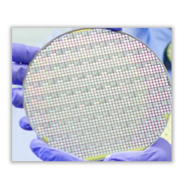
The Process Engineered for manufacturing SiC Electronic devices aim to bring down the cost of SiC-based power device production. Source: North Carolina State University thru EE Times
Silicon carbide (SiC)-a wide-bandgap semiconductor-creates power transistors that are today's premium alternative to silicon power transistors when paired with a diode to provide the lowest-temperature, highest-frequency power devices available. SiC transistors produce 30 percent less heat than silicon power transistors, but thus far SiC's higher performance comes at roughly five times the price of silicon.
North Carolina State University (NCSU) professor Jay Baliga argues that proprietary SiC processes have kept prices high and erected barriers to entry. Looking to lower those barriers with a process that can be licensed at low cost, Baliga and his research colleagues devised the Process Engineered for Manufacturing SiC Electronic-devices or PRESiCE and worked with Texas Instruments' X-Fab to implement it.
PRESiCE is not only a lower-cost alternative to developing your own SiC process but is also more efficient than the old-school, proprietary processes, according to Baliga. Low licensing costs will allow more players to join the competition, thus increasing SiC production. That, in turn, will inevitably drive down prices for SiC, perhaps to only a 50 percent premium over silicon.
Besides running at lower temperatures, SiC power devices can switch at higher frequencies, allowing power electronics to use smaller capacitors, inductors and other passive devices, and ultimately allowing designers to pack more punch into smaller spaces with less weight. Baliga says PRESiCE achieves high yields and tightly controlled properties for the SiC devices it produces.
To prove the concept, the researchers used PRESiCE in TI's X-Fab to fabricate a 1.2kV power supply by manufacturing SiC power MOSFETs, ACCUFETs and junction-barrier-controlled Schottky or JBS rectifiers. A JBS flyback rectifier in the power MOSFET structure created the power JBSFET, which allowed a 40 percent saving in chip area and halved the package count over a silicon-based design.
The PowerAmerica Institute at the Department of Energy provided funding for the research. Baliga's co-authors on the paper are K. Han, J. Harmon, A. Tucker and S. Syed of the NCSU and W. Sung of the State University of New York Polytechnic Institute Colleges of Nanoscale Science.
More Sourcing News
Read Also

关注 “环球资源外贸” 官方微信,获取实时外贸资讯
iOS & Android
iOS & Android(Mainland China)
Copyright © 2026 Publishers Representatives Limited. All rights reserved.