
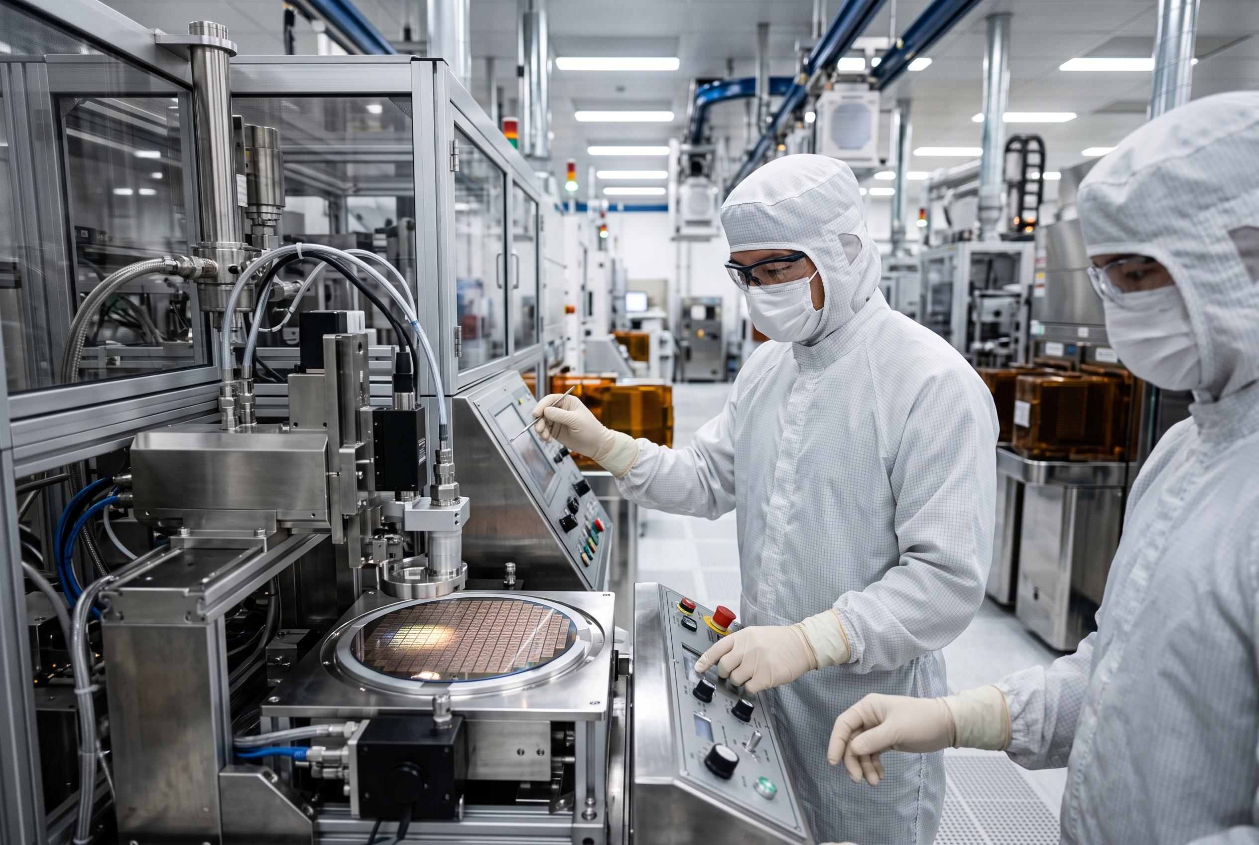
Semiconductor watchers are tracking signs that ASML is developing a die-to-wafer hybrid bonding tool, a move that could deepen its ties with chipmakers and challenge packaging specialist Besi. The technology promises tighter alignment, cleaner processing and a more flexible route to stacking chiplets, although several engineering hurdles remain before it reaches production.
ASML's possible bonding move is bigger than one machine
The most important detail isn't simply that ASML may be building a hybrid bonder. It's that the proposed equipment could extend the company's influence beyond lithography and into the increasingly strategic world of advanced packaging.
ASML's patent activity includes dozens of bonding-related families, with many focused on die-to-wafer processing. Industry coverage from Polaris7 and RootData has also highlighted the company's apparent interest in a system that could compete with Besi's equipment.
That would be a logical progression for ASML. The company has spent years bringing more of the chipmaking process under its roof, from light sources and inspection systems to optics and other critical modules. A bonding platform would give it another way to work closely with customers as chip designs become more three-dimensional.
A track-based design could make bonding more flexible
Traditional die-to-wafer equipment generally picks up a prepared die, aligns it and places it on a wafer. ASML's patent design appears to take a different route. Each die would sit on its own holder and travel around a track, stopping at dedicated stations along the way.
The sequence could include inspection, cleaning, plasma activation, surface measurement and alignment before the die reaches the bonding stage. The approach sounds a little like a miniature production line, but that separation could matter: stations could be sized according to their cycle times rather than forcing every part of the tool to run at the same speed.
SemiAnalysis says this setup could improve station utilization and allow manufacturers to add capacity by adding process stations. It may also be well suited to heterogeneous integration, where different chiplets are combined in one package. For manufacturers juggling several die types, software recipes could provide more flexibility than a rigid, one-product flow.
There is a practical appeal here. Instead of buying another full machine when one operation becomes the bottleneck, a customer might be able to expand the relevant section of the line. That could make a complex tool easier to scale, assuming ASML can keep the entire path clean and synchronized.
Why alignment and particles matter so much
Hybrid bonding joins extremely flat surfaces, often using copper connections without a conventional layer of solder or adhesive between them. That creates a sleek, compact connection, but it leaves little room for error.
A tiny particle can hold surfaces apart and create a void, while even a modest placement error can prevent contacts from lining up. According to SemiAnalysis, alignment becomes especially demanding in die-to-wafer bonding because the process must be repeated across many individual dies.
ASML's experience could be valuable here. Its lithography systems already rely on highly precise sensing, motion control and overlay correction. Patent analysis from the Patent Place and Patsnap also points to continuing research around semiconductor alignment and bonding-related equipment, although patent filings alone don't prove that a commercial product is ready.
Cleanliness is just as important. ASML knows how to control contamination inside demanding lithography systems, but bonding introduces different sources of debris, including particles from singulation and freshly activated surfaces. In other words, the company may have the right habits, but the mess is not exactly the same.
Logic chipmakers may be the first customers
Advanced logic looks like the most natural starting point because die-to-wafer hybrid bonding is already used in some logic products. AMD's V-Cache is a prominent example of stacked logic-related silicon, while TSMC's SoIC technology is pushing toward finer pitches over time.
The tighter the pitch, the less forgiving the bonding process becomes. That makes alignment capability more than a technical talking point. It can directly influence yield, cost and whether a customer can justify the equipment.
TSMC and Intel would be particularly important prospects if ASML moves ahead. The company already has deep relationships with both manufacturers, and its broader roadmap places hybrid bonding alongside front-end technologies such as lithography. A combined workflow could allow bonding data to feed into later exposure steps, reducing the amount of alignment work required on a bonded wafer.
That kind of connection is classic ASML thinking: solve one difficult manufacturing problem, then make the surrounding process more valuable too. It also gives customers another reason to stay within the company's ecosystem.
Besi's lead could face a serious test
Besi currently has the strongest position in die-to-wafer hybrid bonding equipment, with tools in volume production. An ASML challenger wouldn't necessarily displace it overnight, but it could change customer expectations around precision, integration and long-term support.
The pressure may be greatest in advanced logic, where ASML already has established relationships and where customers can afford expensive equipment if it improves yield. Besi's prospects in high-bandwidth memory could also be less certain if adoption takes longer than expected and regional competitors continue improving.
Still, a patent is not a production tool. ASML must prove that its track architecture can handle die transfer, metrology, surface contact and contamination control at commercially useful throughput. The company will also need to qualify the system with demanding customers, and that process can take years.
For now, the most sensible reading is that ASML is exploring a strategically important extension of its technology base. If the machine works as described, hybrid bonding could become less of a standalone packaging step and more of an integrated part of chip manufacturing. That's a powerful idea, even if the engineering reality is considerably less tidy.
Disclaimer: This article may have been created with AI assistance and reviewed by our editorial team. It is provided for general informational purposes only. Readers should verify information independently before relying on this content.
