
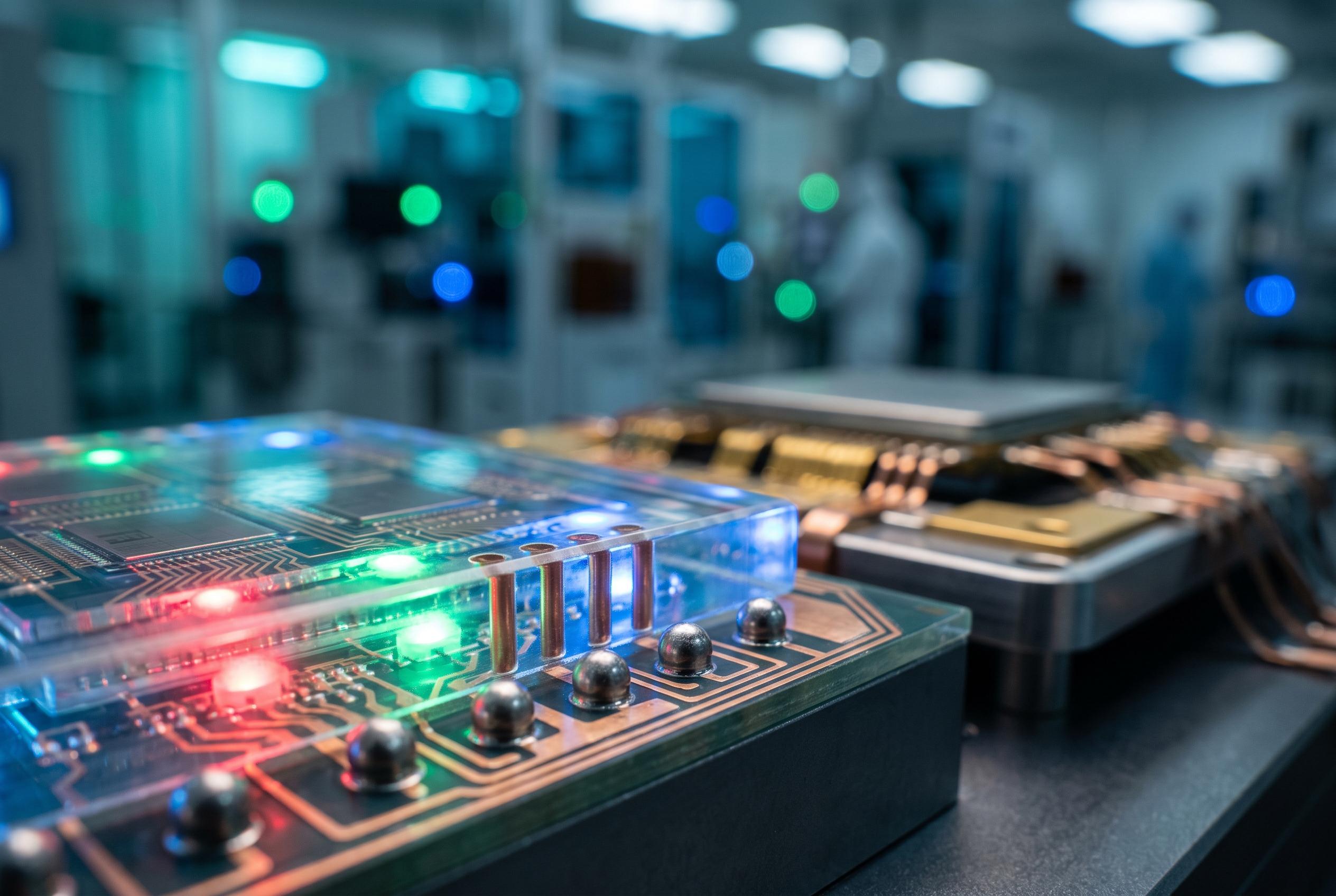
Intel is exploring a glass-based chip package with built-in MicroLEDs, a move that could turn processors into diagnostic displays, illuminated designs, or even components in future optical links. The technology remains a patent concept, but it offers a vivid glimpse at how advanced packaging may become more useful, visible, and surprisingly expressive.
Essential Takeaways
- - MicroLEDs inside the package: Intel’s patent describes placing tiny red, green, and blue emitters in a glass substrate alongside semiconductor dies.
- - Built-in diagnostics: Light patterns could show test results or hardware faults without relying on separate motherboard LEDs.
- - Custom illuminated designs: Future packages might display lettering, logos, or other visual details.
- - Glass enables the connection: Through-Glass Vias, or TGVs, would carry power and signals through the substrate.
- - Optical networking is possible: The same approach could eventually support chip-to-chip optical communication, although the patent doesn’t prove a finished system.
Intel's Chip Package Could Light Up From Within
The most eye-catching part of Intel’s new patent is also the simplest to imagine: a chip package that glows. Rather than placing decorative LEDs around a motherboard, the design embeds MicroLEDs directly into a glass substrate surrounding the semiconductor dies.
According to Tom’s Hardware, the patent outlines RGB MicroLED structures that could produce red, green, and blue light. That could make a processor package show lettering, patterns, or status signals in a way that feels less like traditional PC lighting and more like a tiny built-in display.
There’s a practical angle here, too. Small light sequences could indicate whether a chip passed validation or flag a particular fault. For technicians, that would be far more useful than guessing what a generic motherboard indicator is trying to say.
Glass Packaging Does the Heavy Lifting
The concept depends on more than simply adding lights to a processor. Intel describes cavities and vertical holes formed in glass using laser processing and chemical etching, followed by copper plating to create Through-Glass Vias.
Those vias would provide the electrical paths needed to power the MicroLEDs and communicate with the embedded dies. Global Memory Supply reported that the patent fits into Intel’s broader push towards glass substrates, which are being developed as an alternative to conventional organic packaging materials.
Glass is attractive because it can support large, dense packages while maintaining precise connections between multiple components. It’s a little like swapping a crowded tangle of cables for a carefully planned glass circuit board, although manufacturing at scale remains the hard part.
Could This Make Chip Diagnostics Easier?
Built-in visual feedback may be the most immediately useful application. Instead of adding external LEDs to a board, a package could use a specific colour or pattern to show power, test completion, or a fault condition.
Tom’s Hardware noted that the patent allows for different MicroLED arrangements and package orientations. That flexibility could let Intel place the light-emitting elements where they remain visible during testing, assembly, or servicing.
Still, visibility would depend heavily on the final system design. A large cooler, heat spreader, or protective cover could hide much of the illuminated surface. In a high-performance desktop, the chip might be buried under a substantial heatsink, leaving little room for the light show to escape.
From RGB Branding to Optical Links
The decorative possibilities are easy to picture. A chip could display a product name, an illuminated mark, or a custom pattern, giving manufacturers another way to differentiate premium hardware. For PC builders, it could also reduce the need for separate lighting modules and cables.
The more intriguing possibility is optical communication. Embedded MicroLEDs could potentially act as transmitters inside a co-packaged optics design, sending data through an optical connection rather than relying entirely on electrical pathways.
That’s where caution matters. The patent does not demonstrate a complete optical interconnect, and a working system would also need receivers, optical guides or fibres, and suitable control electronics. Any connection between Intel’s work and MicroLED networking demonstrations from AU Optronics remains speculative rather than confirmed.
Intel Has Been Building Towards Glass Substrates
This patent isn’t an isolated flash of inspiration. Intel has researched glass packaging for more than a decade, beginning work on the material in 2013 and showing early glass-substrate samples in 2023.
The company has also demonstrated a large engineering package using a thick glass core alongside its Embedded Multi-die Interconnect Bridge technology. According to the supplied reporting, that package measured roughly 78 by 77 millimetres and was cut without producing cracks, an important manufacturing milestone.
Intel has separately worked with Lens Technology to refine glass-substrate production processes. That partnership suggests the company is thinking beyond laboratory demonstrations, although commercial products would still depend on cost, yield, cooling, reliability, and supply-chain readiness.
For now, glowing processors belong firmly in the future tense. But the idea points to a broader shift: chip packaging is no longer just a protective shell. It’s becoming an active platform for power delivery, diagnostics, interconnects, and perhaps even a touch of visual personality.
A brighter chip package may be more than decoration, but it’ll need clever cooling and manufacturing before it reaches your PC.
Disclaimer: This article may have been created with AI assistance and reviewed by our editorial team. It is provided for general informational purposes only. Readers should verify information independently before relying on this content.
