
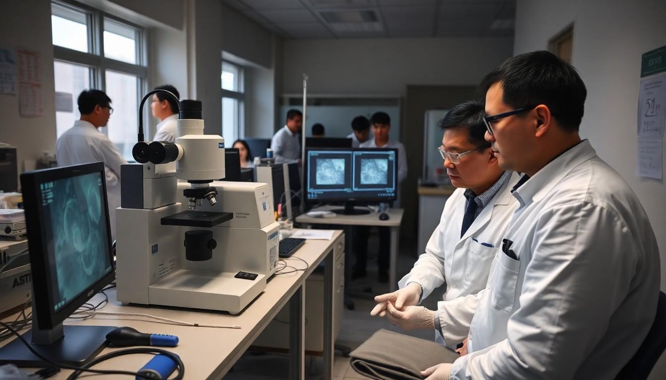
Chipmakers are getting a new tool for tracking elusive defects as JEOL prepares to launch HAXIS, a low-angle ion milling scanning electron microscope, on October 5, 2026. The platform pairs gentle argon-ion sample preparation with passive voltage contrast imaging, helping engineers locate faults in increasingly intricate semiconductor devices without relying as heavily on physical probing.
Essential Takeaways
- - Launch date: JEOL plans to begin HAXIS sales on October 5, 2026.
- - Core technology: Low-angle argon-ion milling creates a flatter, cleaner surface for imaging.
- - Key benefit: Passive voltage contrast can reveal electrical irregularities without direct circuit contact.
- - Why it matters: The combined workflow is designed to shorten failure-analysis turnaround times.
- - Best fit: HAXIS targets advanced chips where dense structures make conventional probing difficult.
A gentler way to expose hidden chip defects
The hardest part of modern chip failure analysis often happens before the microscope takes its first image. Engineers must expose the right device layer without scratching, contaminating, or electrically disturbing the evidence, a delicate job that leaves little room for error.
JEOL's HAXIS tackles that preparation step with Low-Angle Ion Milling, or LIM. The system uses argon ions to remove material at a shallow angle, producing a smooth surface while limiting damage to the underlying structure. According to JEOL's product information, preserving that surface condition is central to obtaining dependable passive voltage contrast results.
That matters because even a technically impressive image can mislead if the sample has been altered along the way. A clean, quiet surface gives analysts a better chance of seeing the fault rather than the preparation artefacts around it.
Why direct probing is becoming less practical
As semiconductor features shrink, reaching individual circuit elements with nano-manipulators becomes increasingly awkward. A probe can also affect the very location being investigated, creating an uncomfortable trade-off between making contact and preserving the evidence.
Passive voltage contrast offers another route. Instead of physically touching a tiny circuit, the microscope detects electrical differences across the prepared surface. JEOL says its work on detectors and sample preparation has helped make PVC observation more stable and repeatable, including on advanced semiconductor structures.
Industry coverage from Tech Capsules describes HAXIS as part of a broader shift toward contact-light failure analysis. That's a sensible direction: when a chip contains more layers, tighter spacing, and more complex wiring, the less an investigation disturbs the sample, the more useful its findings can be.
One workflow could trim the wait for answers
Traditional failure analysis is a relay race. Teams first localise the defect, then perform physical analysis, and finally work backward toward the root cause. If each stage requires separate preparation or equipment, valuable time can disappear between handoffs.
HAXIS brings LIM delayering, scanning electron microscopy, and PVC analysis into one platform. The idea is straightforward but powerful: prepare the surface, inspect it, and identify suspicious electrical behaviour in a connected sequence rather than treating each task as an isolated exercise.
That approach supports quick-turnaround-time failure analysis, a growing priority as chip development cycles tighten. Business Wire reports that the system is intended to speed the move from an electrical failure signal to physical inspection and root-cause investigation.
Argon keeps the process controlled
The choice of argon is more than a technical footnote. As an inert gas, it can provide a controlled milling environment while helping maintain surface quality and limit unwanted reactions during preparation.
For laboratories, operating practicality matters alongside resolution. JEOL says the argon-based process can reduce running costs, while the low-angle technique is designed to retain structural and potential information that might otherwise be lost through more aggressive material removal.
The payoff is not flashy in the way a higher magnification number might be, but it could be more valuable day to day. A repeatable sample is often worth more than a spectacular one-off image, especially when several engineers need to compare results.
What HAXIS means for advanced-chip labs
HAXIS is aimed at a specific pressure point in semiconductor manufacturing: locating faults quickly as devices become harder to access and interpret. It won't replace every stage of physical analysis, but it could make the front end of an investigation more efficient and less invasive.
Conference material from the International Symposium for Testing and Failure Analysis places the technology within the wider conversation around advanced failure-analysis methods. That context is important, because faster localisation can give specialists more time to focus on the difficult question that follows: why did the failure happen?
JEOL's planned October 2026 sales launch will give semiconductor laboratories a chance to assess whether the integrated workflow delivers the promised consistency in real-world investigations. For engineers chasing a microscopic defect through a very complicated chip, even a small reduction in uncertainty can feel like a major breakthrough.
HAXIS could make advanced chip failure analysis cleaner, faster, and easier to repeat.
Source Reference Map
Story idea inspired by: [1]
Sources by paragraph: - Paragraph 1: [2], [5] - Paragraph 2: [2], [3] - Paragraph 3: [2], [4] - Paragraph 4: [3], [6] - Paragraph 5: [2], [4] - Paragraph 6: [2], [5] - Paragraph 7: [2], [6] - Paragraph 8: [2], [4] - Paragraph 9: [2], [3] - Paragraph 10: [2], [5] - Paragraph 11: [2], [4] - Paragraph 12: [2], [7]
