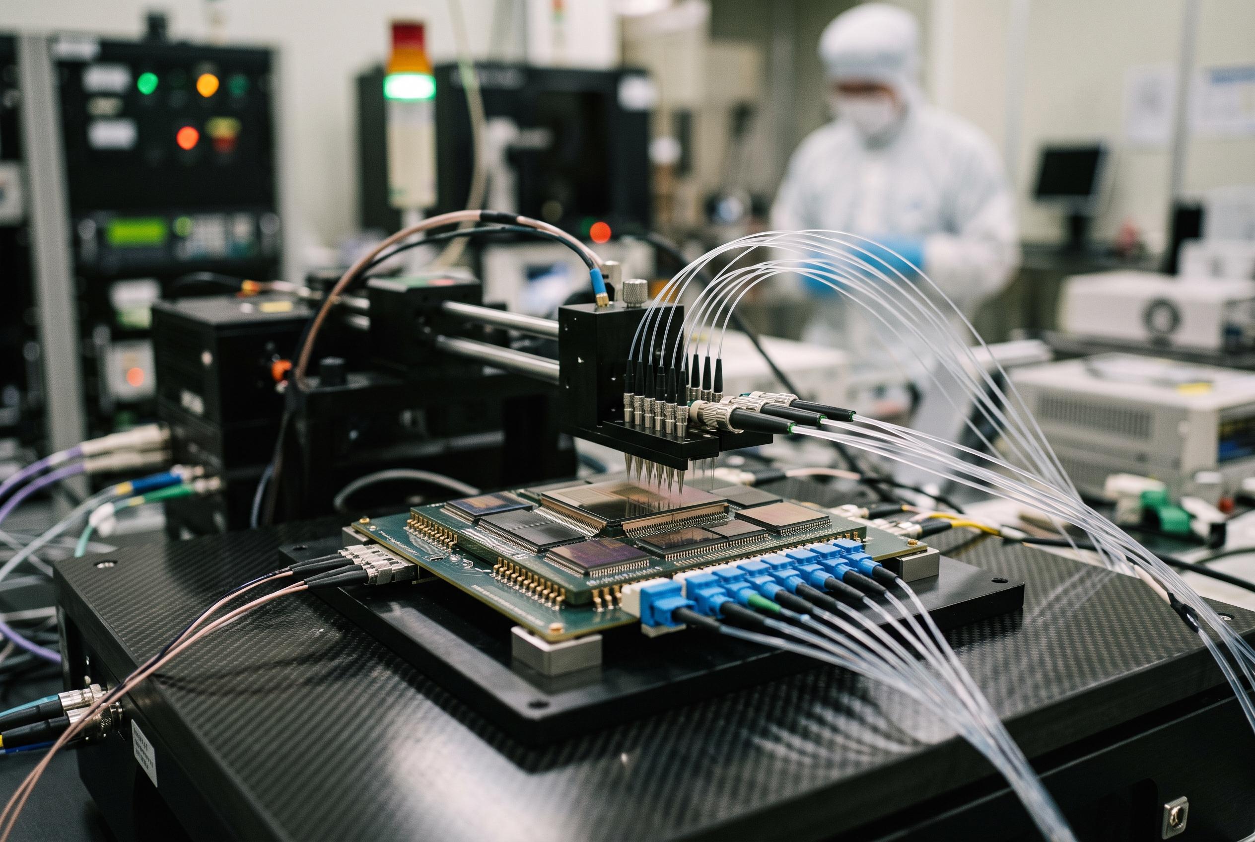
TSMC's 2026 Open Innovation Platform Forum put AI chip design in the spotlight, but the bigger story was cooperation across the entire semiconductor system. From advanced packaging and high-bandwidth memory to optical links and AI-assisted engineering, the company argues that future performance will depend on moving data efficiently, managing heat and making complex designs easier to build.
The next AI chip breakthrough may not be a smaller transistor
The headline from TSMC's 2026 Open Innovation Platform Forum was simple but important: AI performance is now a whole-system problem. Faster logic still matters, but memory access, data movement, heat and power can quickly become the bottlenecks.
That shift changes the feel of semiconductor development. Instead of treating the processor as the star of the show, TSMC's approach places the package, interconnects and design software on the same stage. It's less glamorous than announcing a dramatic new chip name, perhaps, but it's where many of the practical gains will come from.
According to SemiWiki's forum summary, TSMC highlighted applications ranging from robotaxis and humanoid robots to augmented and virtual reality. Those systems demand substantial computing power, but they also need efficient responses in real-world environments, where energy, size and latency matter.
Why TSMC's OIP ecosystem matters
The Open Innovation Platform began as a way to connect customers with design intellectual property and trusted development partners. TSMC now describes it as a much broader network spanning cloud services, 3DFabric packaging and AI-enabled design tools.
The scale is notable. TSMC cites 28 trusted partners, more than 100,000 silicon-verified and production-proven IP offerings, and more than 3,000 engineers working across the journey from early concepts to finished silicon. Those building blocks include processors, memory, interfaces, sensors and security features.
For chip designers, that breadth can save time and reduce risk. A validated component may not sound exciting, but it can spare a team from reinventing a crucial interface or discovering late in development that a supposedly reliable block doesn't behave as expected. In advanced-node manufacturing, that kind of reassurance is worth plenty.
Bigger packages bring memory closer to the action
Advanced packaging was another major theme, particularly as AI accelerators consume more memory and shuffle larger volumes of data. TSMC says its 5.5-times-reticle CoWoS package is already in production and outlined a route toward packages exceeding 14 reticles.
The basic idea is easy to understand. Put computing logic and high-bandwidth memory closer together, and the system can spend less time and energy moving information across longer paths. The engineering is anything but easy, however, because larger packages create fresh challenges involving substrates, assembly, testing, thermals and power delivery.
TSMC also pointed to several memory approaches, including 3D-stacked SRAM, high-bandwidth memory and DRAM integrated with logic. The best option will depend on the workload. Training, inference and agentic AI applications don't all make the same demands, so a single memory recipe won't suit every future system.
Faster chips need faster ways to move data
Connectivity is becoming just as important as computation. TSMC says a 200-gigabit-per-second micro-ring modulator based on its COUPE technology is in production, while future work includes 400Gbps modulation, multiple wavelengths and fiber-array integration.
The company has outlined a long-term target of four terabits per second per millimeter by 2030. That figure is a reminder that even a powerful processor can be held back if data can't reach it quickly and efficiently.
This is where optical links become especially interesting. As AI systems grow, electrical connections face increasing pressure from distance, power consumption and signal integrity. Optical technology won't replace every connection overnight, but it offers a promising route for high-capacity links inside and around increasingly complex systems.
Can AI help engineers build the next AI chip?
TSMC also described AI as a design tool, not merely the workload that chipmakers are trying to support. The company says more than 70% of the forum's papers either use AI methods or focus on AI applications, reflecting how quickly the technology is entering engineering workflows.
Its proposed AI Design Kit, or ADK, would move design enablement toward an agentic model. In practical terms, that could mean AI systems using design information, training material and established workflows to assist with tasks from technology co-optimization through implementation and signoff.
The promise is attractive: higher productivity, fewer repetitive steps and shorter development cycles. Still, chip design is not a setting where plausible answers are good enough. These systems will need careful validation, traceability and human oversight before engineers can trust them with critical decisions.
The practical challenge is keeping the system balanced
TSMC's broader message is that no single improvement will carry the next generation of AI hardware. Better logic needs efficient memory. Larger packages need stronger thermal solutions. More computing capacity needs faster interconnects, and every improvement has to fit within a realistic power budget.
That explains the emphasis on collaboration among EDA companies, IP suppliers, memory manufacturers, assembly and test specialists, substrate makers and original design manufacturers. The future chip may be designed by one company, assembled through several partners and optimized across an entire data-center stack.
For businesses choosing a semiconductor platform, the lesson is useful: look beyond headline process-node claims. Ask how the design ecosystem handles packaging, memory, verification, thermal planning and software-assisted development. Those details can determine whether an ambitious AI product becomes a working system or an expensive science project.
TSMC's forum ultimately presents collaboration as a performance technology in its own right. The next leap in AI hardware may come from a quieter, more coordinated stack rather than one spectacular component.
It's a reminder that the fastest chip is only as useful as the system built around it.
Disclaimer: This article may have been created with AI assistance and reviewed by our editorial team. It is provided for general informational purposes only. Readers should verify information independently before relying on this content.