


HDI PCBs find widespread use in smartphones, tablets, wearable devices, medical instruments, aerospace avionics and automotive electronics – essentially any application where miniaturization, signal integrity and reliability are paramount. As devices continue to shrink, they remain indispensable.
A significant advancement in PCB technology, HDI boards enable designers to pack more functionality into smaller form factors. By utilizing microvias, blind and buried vias, and finer trace widths, these achieve greater wiring density per unit area than conventional PCBs.
HDI PCBs are typically constructed using advanced materials suited to their demanding electrical and thermal requirements. Standard high-Tg FR-4 laminates remain common for many applications, while more performance-critical designs may employ materials such as BT resin, polyimide or low-loss PTFE-based substrates. Prepreg and copper foil thicknesses are carefully selected to support the fine features that define HDI construction.
Layer counts in HDI boards vary widely depending on complexity. Simple designs may use four to six layers with a single buildup of microvias on each side, while advanced configurations can exceed 20 layers using multiple sequential lamination cycles. The notation "1+N+1" or "2+N+2" is commonly used to describe the number of buildup layers surrounding the core.
Surface finishes applied to these PCBs include ENIG, ENEPIG, OSP and immersion silver or tin, the choice of which depends on solderability requirements and component compatibility.
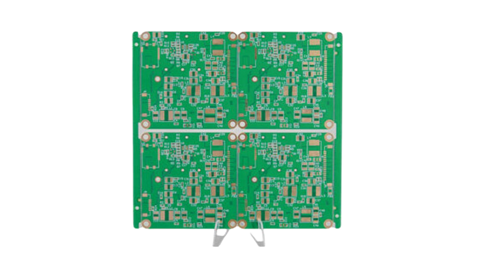
HDI PCB, up to 48 layers
Company: China Dragon Electronic Industrial Co. Ltd
China Dragon offers the CDC-6612, an HDI PCB which can be made with up to 48 layers, 0.5 to 4oz copper, FR-4, high-Tg FR-4, high-frequency, aluminum or flexible laminate base and HASL, lead-free HASL, immersion gold, tin or silver, hard gold, flash gold or OSP surface treatment. The minimum line width and spacing is 3mil and the board thickness is 0.1 to 4mm±10 percent. The lead time is provided on direct inquiry.
MOQ: 1 unit
HDI PCB for high-frequency applications
Company: Shenzhen Gaofuheng Electric Technology Co. Ltd
The HFP-002 from Shenzhen Gaofuheng is a gold-impregnated HDI PCB for high-frequency applications. It has eight layers, high-Tg laminate base and a Rogers substrate. The supplier accepts small orders.
Lead time: 10 to 14 days
Eight-layer HDI PCB
Company: Shenzhen GK Circuits Co. Ltd
From Shenzhen GK, the MS-2207-1226 is an eight-layer HDI PCB with an FR-4 laminate base and OSP, ENIG or lead-free HASL surface treatment. It has an inner trace width and space of 3mil or 0.076mm and 3.2mil or 0.081mm while the outer measurements are 3mil or 0.076mm and 3.8mil or 0.097mm. The minimum size of mechanically drilled holes is 0.25mm and that of laser drilled holes is 0.1mm. The finished thickness of this RoHS-compliant PCB is 1.6mm. The supplier accepts small orders.
Lead time: 5 to 30 days
Custom-made HDI PCB
Company: Shenzhen Merrillchip Electronics Co. Ltd
Shenzhen Merrillchip supplies HDI PCBs based on custom specifications, such as model HDI PCB for Medical Devices. Single-, double- and multilayer units can be made with an immersion silver or tin or other surface treatment options. The supplier accepts small orders.
Lead time: 3 to 7 days
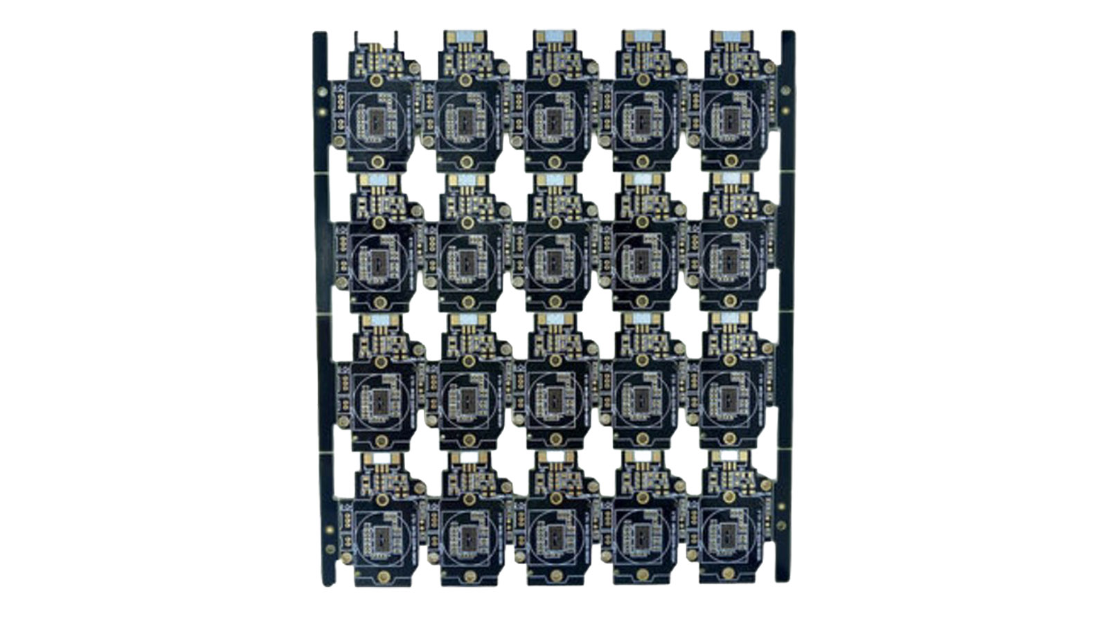
Aluminum-bonded HDI PCB
Company: Shenzhen Provision Co. Ltd
The N539-T-4867 from Shenzhen Provision is an aluminum-bonded HDI PCB for LED modules. It can be made to have up to 20 layers, FR-4, Rogers or CEM-3 base material, 0.5 to 6oz copper, ENIG, immersion tin, OSP or HASL surface treatment and green, red, blue, black or white solder mask. The minimum size of mechanically drilled holes is 0.15mm.
MOQ: 1,000 units
Lead time: 7 to 20 days
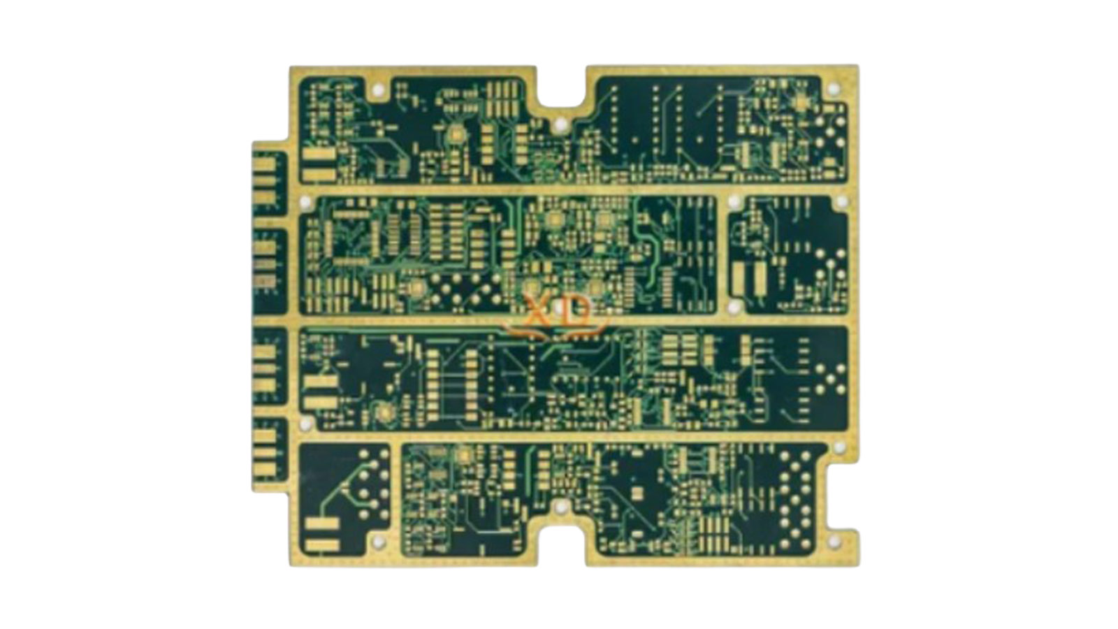
HDI PCB, up to 12 layers
Company: Shenzhen XinDaXing Electric Technology Co. Ltd
Shenzhen XinDaXing’s model pcbgate260203179 is an HDI PCB for 50G SFP28 optical transceivers. It is available with two to 12 layers, with ≥3.5mil minimum spacing. This board uses Megtron 6 or 7, Rogers or other material, immersion silver+OSP surface treatment, and 0.5 to 1oz copper on the inner and outer layers and 2oz on the power layer. It has impedance control of less than 50ohms±5 percent. Board thickness is 0.8 to 1.6mm±0.1mm. The MOQ is provided on direct inquiry.
Lead time: 5 to 7 days