
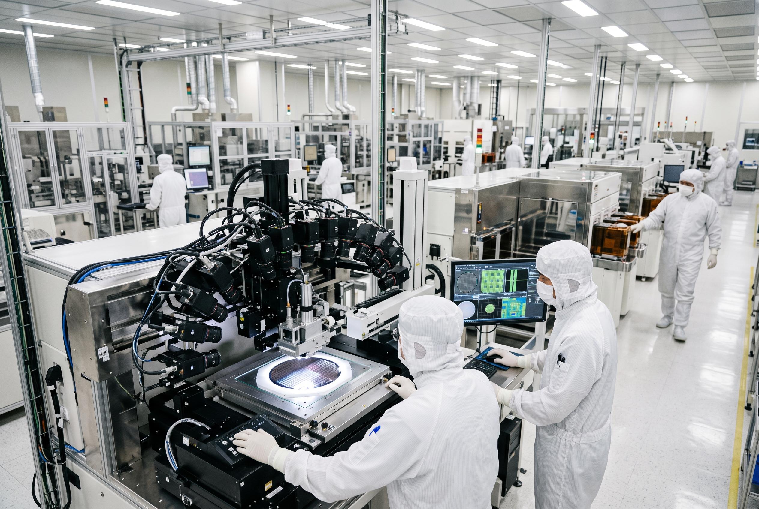
Taiwan is stepping up its semiconductor inspection game with array-based 3D technology designed for large, precise areas. Developed by ITRI with local industry partners, the system uses multiple cameras at once, helping chip manufacturers and packaging companies inspect increasingly complex structures faster while reducing reliance on overseas equipment suppliers.
Advanced chips need a sharper set of eyes
As AI processors become more powerful, the structures around them are also becoming more intricate. Tiny differences in height, alignment, or surface condition can affect how a component performs, making inspection less of a final check and more of a critical part of production.
The challenge is that traditional single-camera 2D systems can struggle when manufacturers need all three things at once: wide coverage, fine detail, and fast throughput. According to ITRI, its new array-based 3D inspection approach is intended to address that trade-off with simultaneous imaging across multiple cameras.
That sounds like a technical upgrade, but the practical effect is easier to understand. More of the surface can be measured in one pass, with depth information helping engineers spot issues that a flat image could miss.
Why 3D inspection matters for semiconductor packaging
Advanced packaging brings several components and layers together in compact formats. That density creates more opportunities for small defects, uneven surfaces, or alignment problems to hide in places that are difficult to assess with conventional vision systems.
ITRI developed the technology in partnership with Taiwanese companies, with the goal of supporting semiconductor manufacturers, assembly houses, and testing providers. Industry suppliers such as WisePioneer already offer equipment for wafer, FOUP, and FOSB inspection, showing how specialised the inspection market has become.
The broader shift is clear: inspection is moving beyond simply asking whether a surface looks right. Manufacturers increasingly need detailed measurements that can support process control, traceability, and faster decisions on the production line.
Multiple cameras could help manufacturers cover more ground
The system’s array design is its most important feature. Rather than relying on a single camera to capture a large area or repeatedly repositioning one imaging unit, several cameras work together during inspection.
That arrangement can improve efficiency when manufacturers are dealing with larger wafers, complex packaging formats, or high-volume production. It also gives equipment makers more flexibility to tailor inspection systems to particular processes, rather than forcing every customer into the same configuration.
There’s a quiet but important benefit here, too. Faster inspection can help reduce bottlenecks, while better three-dimensional data may give engineers more confidence when they’re evaluating delicate or expensive components.
Validation gives the technology more weight
Precision claims matter in semiconductor manufacturing, where a small measurement error can have costly consequences. ITRI says the array-based 3D inspection technology was validated using reference standards from NIST, the US agency known for developing measurement standards and supporting accurate industrial testing.
That validation doesn’t mean every production line will see identical results. Real-world performance still depends on the equipment configuration, the material being inspected, lighting, calibration, and the requirements of each factory. Still, using recognised reference standards gives potential adopters a clearer basis for judging accuracy.
For buyers comparing semiconductor inspection and metrology equipment, the lesson is practical: look beyond camera count or headline resolution. Ask how the system is calibrated, what standards support its measurements, and whether it can integrate with existing manufacturing and quality-control workflows.
Taiwan wants more control over critical inspection tools
Advanced inspection equipment has traditionally depended heavily on overseas suppliers, particularly as chip structures have grown more demanding. ITRI’s project reflects Taiwan’s effort to build more domestic capability around the semiconductor supply chain, not just in chip production itself.
Local development can also make it easier to customise equipment for Taiwanese manufacturers. Semiconductor companies often need specialised formats, software connections, and service support, so a closer relationship between technology developers and equipment makers may shorten the path from prototype to factory floor.
The technology is still part of a wider ecosystem rather than a single solution. Companies such as Semiconductor Equipment Corporation and Chunson represent the kind of industrial network that can help turn research advances into practical tools, although adoption will depend on reliability, cost, throughput, and integration.
If the approach delivers on those fronts, Taiwan’s inspection equipment sector could become a more visible part of the global semiconductor story. After all, the smallest details often decide whether the biggest chips succeed.
It's a small-looking inspection upgrade with potentially large consequences for chipmaking efficiency.
