
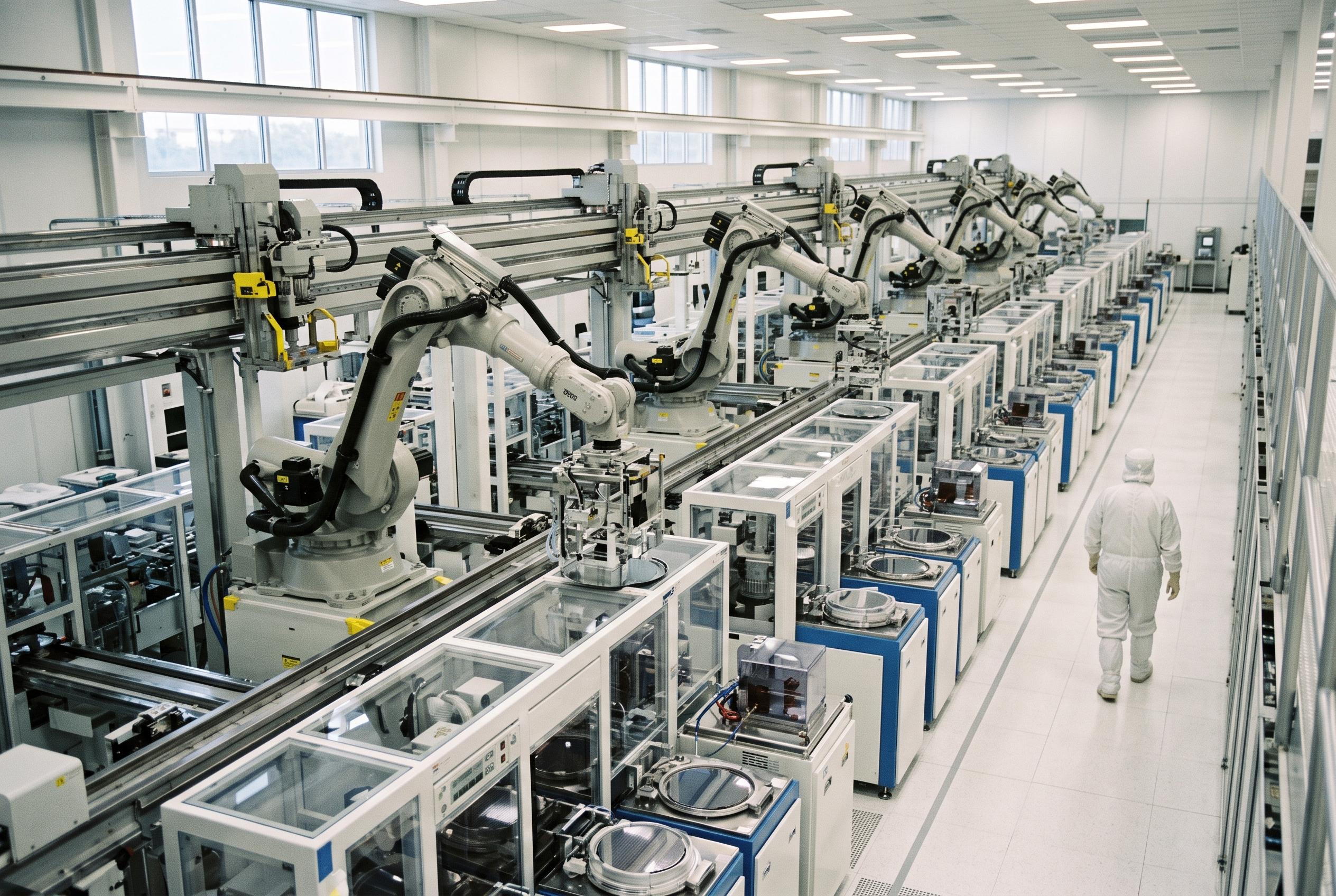
As complexity in semiconductor design surges, industry shifts towards modular chiplet architecture, promising enhanced flexibility, cost-efficiency, and faster innovation in next-generation computing systems.
Chiplet Architecture: Redefining Semiconductor Design, Manufacturing, and Sourcing
As semiconductor complexity soars and market demands diversify, the industry is witnessing a transformative shift toward chiplet architecture, a modular approach that promises to redefine how complex computing systems are designed, built, and sourced. Unlike traditional monolithic system-on-chip (SoC) designs where all functions are integrated into a single silicon die, chiplets are smaller, independently manufactured silicon blocks that can be combined within a single package. This shift addresses escalating development costs, physical limitations of advanced nodes, and the growing need for customization and scalability.
What Are Chiplets and Why Do They Matter?
Chiplets are discrete functional units, processing cores, memory blocks, I/O interfaces, that can be mixed and matched across different silicon process nodes and intellectual property (IP) blocks. Traditional SoCs require a unified manufacturing process, often at the cutting edge, combining all functions onto a single die. This monolithic approach incurs rising complexity, longer development cycles, and higher costs due to design overhead and lower yields as chips grow larger.
Chiplet architecture’s modularity lets semiconductor manufacturers combine components fabricated on different nodes, say, combining a high-performance CPU core on a 5nm process with analog or I/O components made on a more mature, cost-effective 22nm process. This heterogeneous integration is achieved through advanced packaging technologies and high-speed die-to-die interconnects, enabling seamless communication within a single package that functions as one system.
Drivers Fueling the Chiplet Revolution
Several forces are converging to push chiplets from concept to mainstream adoption:
- - Rising Chip Complexity: As system requirements balloon, integrating all components monolithically becomes impractical and inefficient.
- - Escalating Development Costs: Advanced node development costs can exceed hundreds of millions, amplifying risks on large, monolithic chips.
- - Advanced-Node Limitations: Physical scaling at sub-5nm nodes faces technical hurdles like variability and yield challenges.
- - Demand for Customization and Scalability: Chiplets empower OEMs and system integrators to flexibly assemble tailored solutions without redesigning entire SoCs.
From an Industry and Buyer Perspective
Chiplets allow manufacturers to orchestrate a “mix-and-match” strategy, combining best-in-class IP blocks and process nodes within one package. Advanced packaging techniques, such as 2.5D interposers, fan-out wafer-level packaging (FOWLP), and silicon interposers, facilitate dense, high-speed die-to-die interconnects that minimize latency and power consumption.
This yields significant advantages:
- - Development Time and Manufacturing Flexibility: Reusing verified chiplets shortens validation and design cycles while allowing diversified supply chains.
- - Performance and Cost: Optimizing each chiplet on the best-suited process node balances peak performance with cost-efficiency.
- - IP Reuse and Node Independence: Reduces dependency on a single foundry or process technology, mitigating supply chain risks.
Yet, challenges remain. Thermal management grows complex as multiple active die operate in close proximity. Power efficiency must be carefully engineered to avoid bottlenecks. Interoperability among heterogeneous chiplets requires robust standards to enable seamless integration. Testing and yield optimization become multidimensional, demanding innovative solutions in design-for-test and packaging. Packaging complexity itself escalates with denser interconnects and multi-die stackups.
Industry initiatives like the Universal Chiplet Interconnect Express (UCIe) standard have become pivotal. UCIe defines open, standardized interfaces to ensure broad compatibility, accelerate ecosystem maturity, and reduce integration risk. This interoperability is crucial for semiconductor suppliers, OEMs, and electronics manufacturers who must collaborate across supply chains in sourcing chiplet components.
Real-World Adoption
Chiplet designs are proving their worth in demanding sectors. AI accelerators leverage chiplets to combine compute-heavy cores with high-bandwidth memory on tailored nodes. Data centers and high-performance computing systems benefit from scalable, modular architectures that optimize power and performance. Networking and automotive electronics demand highly reliable, customizable chiplets that meet rigorous standards. Edge computing systems adopt chiplets for compact, low-power modular solutions.
Implications for Sourcing and Strategy
For sourcing teams and corporate buyers, chiplet adoption introduces both opportunity and complexity. Evaluating chiplet-based solutions requires scrutiny of a supplier’s packaging capabilities, IP portfolio integration expertise, and adherence to emerging standards. Flexibility to source from multiple foundries and packaging providers becomes a strategic asset, diversifying risk and enhancing innovation.
Looking Ahead
Chiplet architecture signals a new paradigm, shifting semiconductor design and sourcing from monolithic, single-vendor dependency toward an ecosystem-driven, modular assembly model. This approach inspires greater design flexibility, fostering cross-vendor collaboration and unlocking new supplier ecosystems specializing in chiplets, advanced packaging, and IP integration.
The semiconductor supply chain is poised for evolution: advanced packaging capacity will be a critical bottleneck, urging collaboration between IDM, fabless, and foundry players. Sourcing strategies will pivot to embrace modular component acquisition over all-in-one silicon solutions.
As chiplet architecture matures, it promises to democratize semiconductor innovation, enabling companies to rapidly deploy next-generation computing systems, tailor-fit to diverse and evolving requirements across AI, data center, automotive, and edge markets. Embracing this paradigm means rethinking not just chip design, but the entire approach to building and sourcing complex computing technology for the future.
