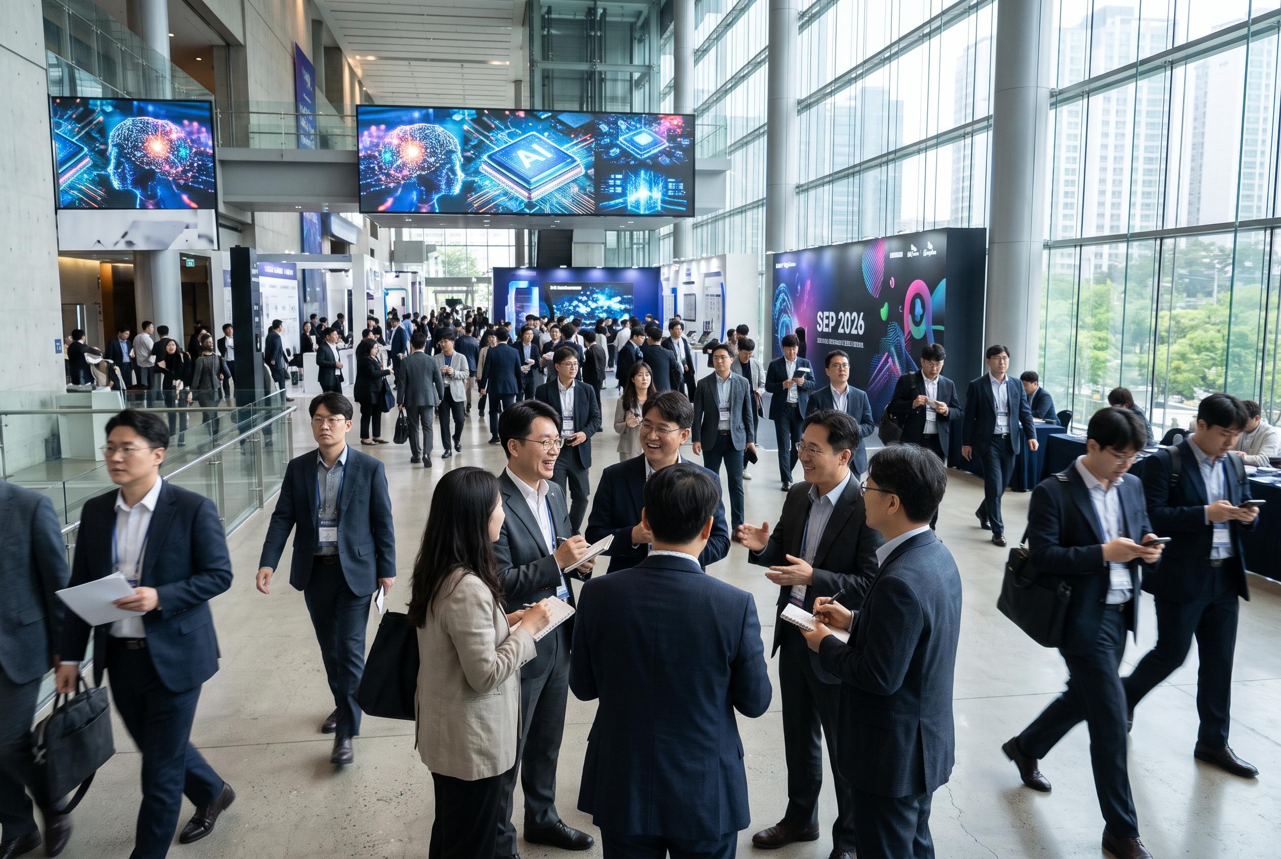
Visitors at Seoul’s SEDEX 2026 are getting a preview of how Samsung Electronics and SK Hynix see AI’s next chapter unfolding. Their focus is shifting beyond faster chips toward HBM4 and HBM4E memory, smarter manufacturing, and lower power use, because the biggest limits on AI may soon be energy and data movement.
AI Chipmaking Is Becoming a Factory-Wide Operation
The most striking message from the event is that AI isn't just creating demand for semiconductors. It's also changing how those semiconductors are designed and made.
Samsung Electronics says it uses techniques including reinforcement learning and genetic algorithms to automate repetitive design decisions, such as adjusting transistor dimensions and spotting possible design-rule problems early. The company has said these tools can cut design time substantially in some cases. Samsung's broader AI semiconductor work has also included smarter process control, virtual factory models, and automated analysis of manufacturing data.
That matters because chip development is becoming painfully complex. A small improvement in design speed can help companies bring products to market sooner, while faster detection of defects can protect expensive production capacity. Samsung's technology updates show an industry moving toward AI agents that connect design, engineering, and manufacturing rather than treating each stage as a separate island.
HBM4 and HBM4E Put Memory Centre Stage
For years, the public conversation around AI chips focused mainly on processors. Now the spotlight is moving to the memory sitting alongside them.
High-bandwidth memory, or HBM, stacks multiple memory layers and connects them closely to AI accelerators. That arrangement allows large volumes of data to move quickly, which is essential for training and running demanding AI models. Samsung has highlighted commercial HBM4 development and next-generation HBM4E work, while SK Hynix has announced samples of 12-layer HBM4E, according to company updates.
The progression from HBM3E to HBM4 and HBM4E is about more than headline speed. Capacity, thermal behaviour, packaging, reliability, and compatibility with advanced processors all matter. Samsung's HBM announcements also point to a market increasingly shaped by close collaboration with AI chip designers, including Nvidia, because memory works best when it is designed as part of the wider computing system.
Why the “Energy Wall” Could Slow AI Growth
Faster memory is useful, but it comes with a catch: moving data consumes energy. As AI data centers expand, electricity demand is becoming a practical constraint rather than a line item quietly buried in operating costs.
SK Hynix has framed the next challenge as an energy wall. Its proposed answers include improving HBM bandwidth per watt, shortening the distance between memory and computing units, and developing architectures tuned to particular workloads. In plain English, the goal is to get more useful AI work from every unit of power.
This is where 3D integration becomes especially interesting. Samsung has showcased longer-term 3D memory concepts that could bring processing and memory into tighter arrangements, potentially reducing the energy lost while data travels between components. The technology is still part of a fast-moving development story, but the direction is clear: future AI performance will be judged by efficiency as well as raw speed.
Samsung and SK Hynix Are Chasing Different Edges
Samsung's pitch is broad. It is combining memory research with AI-assisted chip design, advanced manufacturing, packaging, and digital twins that replicate production facilities in software. That approach could help the company improve several stages of the semiconductor pipeline at once.
SK Hynix, meanwhile, is especially focused on its central role as a memory supplier. Its HBM strategy centres on higher capacity, faster data transfer, and closer alignment with the processors driving AI workloads. Its HBM4E sample announcements underline how quickly the company is trying to move from one generation to the next.
For buyers of AI infrastructure, the distinction is useful. A faster memory product isn't automatically the best choice if it raises heat, complicates packaging, or consumes too much electricity. The winning solution will likely be the one that balances performance, supply, durability, and power efficiency.
What This Means for the Next AI Hardware Cycle
The semiconductor industry has already moved through major demand waves led by personal computers, smartphones, and cloud computing. AI is creating another one, but this cycle looks more tightly connected to infrastructure. Every jump in model size and usage puts pressure on processors, memory, networking, cooling, and electricity.
That makes events such as Seoul's Smart Energy Plus especially relevant. The discussions are no longer limited to whether a chip can run an AI model. They increasingly ask whether data centers can power, cool, and scale that model affordably. Samsung's technology showcases and SK Hynix's HBM roadmap both suggest that memory and energy efficiency will sit near the centre of that debate.
For everyday technology users, the changes may be invisible at first. But they could eventually influence how quickly AI services respond, how much data centers cost to operate, and whether new AI features can expand without pushing electricity demand too far. It's a quiet hardware race, but its effects may be felt everywhere.
The future of AI won't be decided by speed alone; it will be won by chips that move data intelligently and use power carefully.
Disclaimer: This article may have been created with AI assistance and reviewed by our editorial team. It is provided for general informational purposes only. Readers should verify information independently before relying on this content.