Download App
Better Online and Trade Show Sourcing Experiences.Scan the QR code to download.
Learn More
Hot Topics
by Vianie Li & Cecile de Veyra
Over the years, miniaturization in electronics has been addressing signal, heat and interference issues associated with ultrasmall components closely mounted together. Breakthroughs have paved the way for more compact but powerful devices. As this trend is still driving product development across categories, PCB solutions such as HDI and flexible types are growing in popularity.
HDI PCBs, which fall under the multilayer category, offer size and weight advantages as they have a greater number of interconnections per unit area than ordinary boards. They are found in a range of medical devices, from lab equipment, including probes, to implants such as pacemakers.
Besides being thin, lightweight and bendable, flexible PCBs have high wiring density. They are used in LED lighting, particularly strip types, mobile phones, and wearable products from smart devices to sensor-equipped clothing and accessories. Rechargeable batteries with flexible circuitry are also an application. In the medical field, flexible boards are found in wearables, implants, hearing assistive devices, diagnostic equipment such as MRIs, CT and ultrasound scans, and portable monitoring equipment.
The global HDI PCB market is expected to increase to $25.72 billion by 2026, posting 11.5 percent CAGR from 2021, according to 360 Research Reports. In 2020, it reached $13.39 billion. Flexible PCBs, meanwhile, will be about $27 billion by the end of 2022 based on Allied Market Research’s projection.
Chinese multilayer PCB suppliers interviewed by Global Sources believe that future HDI boards will have a minimum line width and spacing of 60µm or even as fine as 40µm or below. In current releases on the market, the range starts from less than 100µm. These manufacturers also say that R&D will shift focus from 2+N+2 to 3+N+3 or any-layer builds in the next one or two years. As for flexible PCBs, they anticipate product development will trend toward superthinness, greater flexibility and low price in the coming years.
Growth catalysts for these PCB categories are 5G communication and the Internet of Things, which require multilayer PCBs with a high density and complexity. According to Chinese market research site Industry Information Net, HDI PCBs already accounted for 40 percent of boards used in mobile terminals worldwide and flexible types 30 percent.
In China, a number of initiatives that focus on the manufacture of HDI PCBs have been launched recently.
Huizhou China Eagle began trial operations at its new factory in March 2021, with a target annual production value of $140 million to $170 million once fully up and running.
Shenzhen Kinwong, meanwhile, has invested $730 million in two facilities in Zhuhai, one for high-layer and the other for HDI boards, and both started mass manufacturing in 2021. Annual capacity is 1.2 million square meters for multilayer PCBs and 600,000sqm for HDI units. The multilayer PCBs have an average layer count of 12, with the highest at 40, and are designed for communications, server, automotive and industrial control applications. For any-layer HDI variants, production emphasis is on up to 16 layers.
Despite the pandemic, the PCB industry reached a production value of $65.2 billion in 2020, up by 6.36 percent YoY, according to Prismark, and China accounted for 53.8 percent. In terms of shipments worldwide, multilayer and flexible boards were the top finishers, with respective shares of 37.39 and 20.01 percent during the same year.
Based on Qianzhan Industry Institute’s forecast, rising demand in various electronics categories will bring up worldwide PCB production value to $69.1 billion by end-2022 and $78 billion by 2026. Multilayer boards are expected to continue to take the lead.
This has encouraged most Chinese multilayer PCB suppliers to increase their output in 2021, according to companies interviewed. To double its capacity, Shenzhen Hopesearch PCB Mfg Co. Ltd acquired several items of advanced production equipment for its existing factory and built a new factory in Pingxiang, Jiangsu province, in 2021. It will increase production twofold in the months ahead and raise the allocation for boards with more than eight layers.
More than a thousand companies make up the manufacturing pool for multilayer PCBs in China, two-thirds of which are homegrown enterprises with small or midsize operations.
More than half of these companies are found in Shenzhen, Dongguan, Zhongshan and Guangzhou, with many others in Suzhou, Kunshan and Changzhou.
Major players include Avary Holding, Suzhou DSBJ and Shennan Circuits. Other suppliers shipping globally from production facilities in China are Tripod Technology, Zhen Ding Tech, Compeq and Mektec.
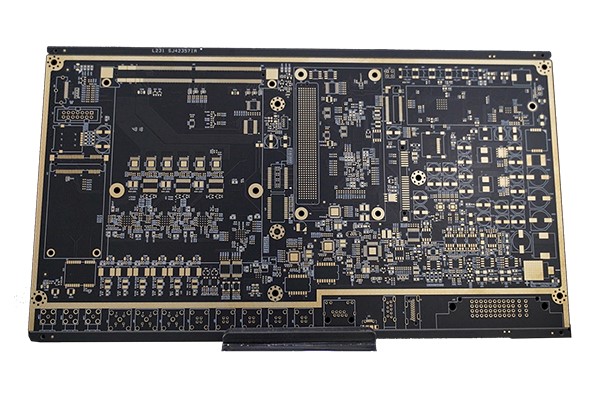
Multilayer PCBs are available from Chinese manufacturers in rigid, flexible and rigid-flex kinds with a maximum count of 40 layers, with the most widely shipped having four, six, eight and 12 layers.
These boards are RoHS-compliant. They have a minimum line width and spacing of 3mil, smallest hole size of 0.2mm, copper of 0.5 to 7oz and board thickness ranging from 0.21 to 7mm. Common surface finishes include immersion gold, silver and tin, ENIG, HAL and lead-free HAL.
Copper-clad laminates represent more than 40 percent of multilayer PCB production costs. FR-4, CEM-1, CEM-3 polyimide, Rogers and high-Tg are some of the choices. Together with ink and adhesive, these materials are sourced from domestic or foreign providers, depending on buyer preferences.
Outlay for these manufacturing inputs rose slightly in 2021, prompting many companies to increase prices by 5 percent. Suppliers interviewed are anticipating a different situation in the coming months, predicting costs and quotes will stabilize.
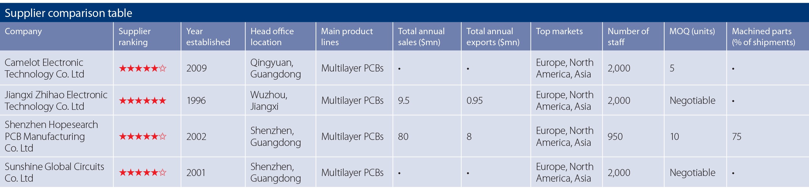
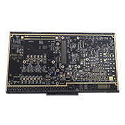
Camelot Electronic Technology Co. Ltd’s D541001A0 is a 16-layer PCB using an FR-4 base. It has 0.2mm minimum holes, green solder mask, white silk-screening and immersion gold surface finish. Board thickness is 1.2mm and size 205x100mm.
The negotiable order quantity has a seven-day lead time.
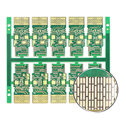
This 20-layer PCB from Jiangxi Zhihao Electronic Technology Co. Ltd has 2oz copper thickness, 4mil minimum line width and spacing, ENIG surface finish and 3mm board thickness.
The order quantity is negotiable. Delivery takes seven days.
For industrial control applications, Shenzhen Hopesearch PCB Mfg Co. Ltd’s 10-layer PCB uses a high-Tg FR-4 material, and has 210µm copper, 0.25mm minimum holes, 3mil and 4mil minimum line width and spacing, and immersion gold surface finish. Board size is 326x242mm, with finished thickness of 1.6±0.16mm. Impedance control is 55±5ohm.
The 10-unit minimum order has a lead time of seven days.
The 400Gbps QSFP-DD model from Sunshine Global Circuits Co. Ltd is a 10-layer PCB for use in optical modules. It uses a Megtron6 material with an ENEPIG surface finish.
The order quantity is negotiable. Delivery is within seven days.
PCB manufacturers struggle to shift Chinese mainland operations
Rigid-flex PCB with electrolytic gold
Multilayer HDI PCB for mobile phones
PCB assembly capability for up to 01005 components
Multilayer PCBs going high density & high complexity
Multilayer PCB production moving toward additive technologies
Application Watch: Future of flexible PCBs for wearables in additive printing technology
More Sourcing News
Read Also

关注 “环球资源外贸” 官方微信,获取实时外贸资讯
iOS & Android
iOS & Android(Mainland China)
Copyright © 2026 Publishers Representatives Limited. All rights reserved.