
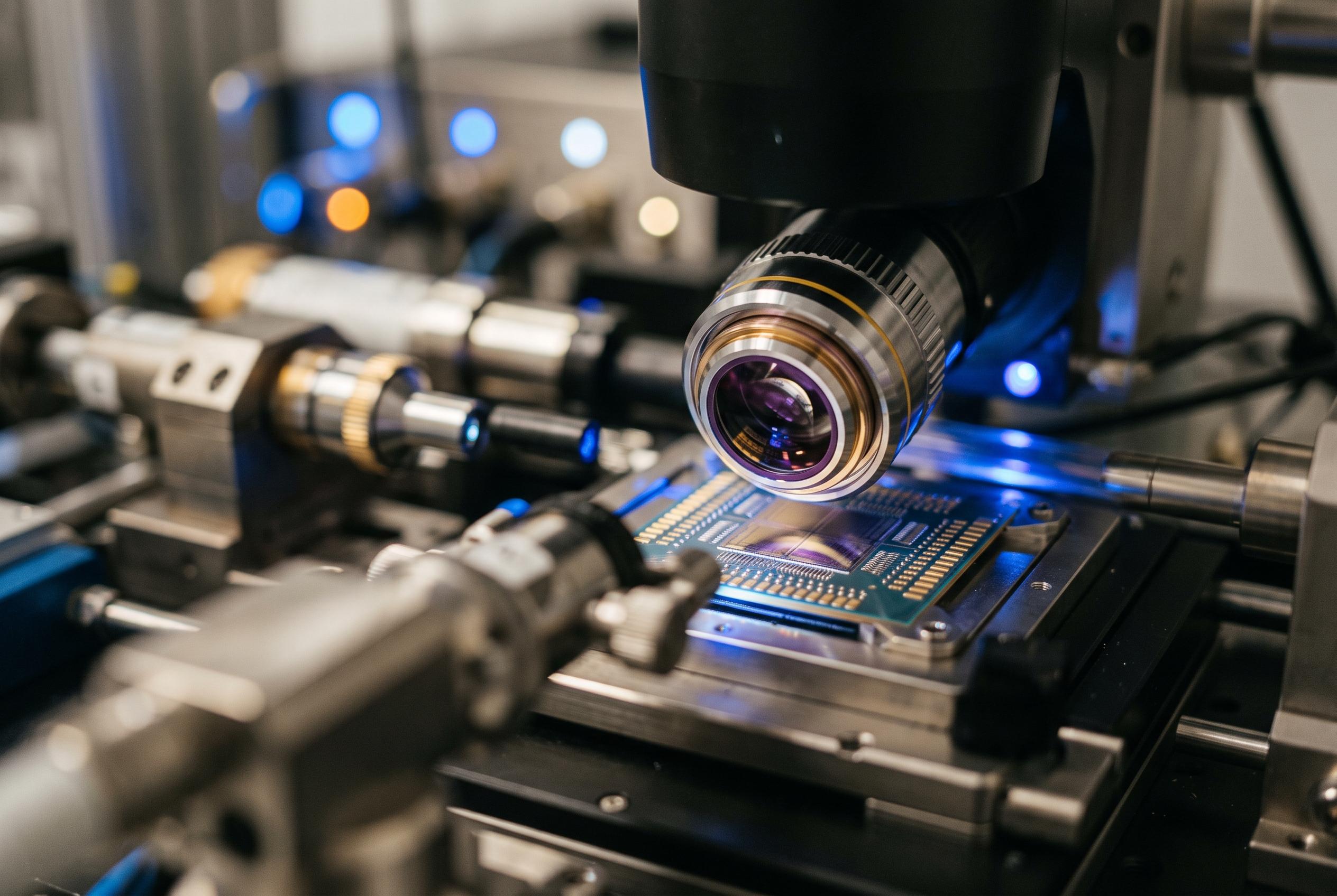
Chipmakers are getting a new way to track elusive defects in AI chiplets, 3D packages, and High Bandwidth Memory. Hamamatsu Photonics' iPHEMOS-DDX combines seven analysis methods in one inverted emission microscope, helping laboratories move from fault detection to diagnosis with less equipment shuffling and fewer workflow interruptions.
Essential Takeaways
- - Seven tools, one platform: The iPHEMOS-DDX brings together electrical, thermal, optical, and time-domain analysis methods.
- - Built for advanced packaging: It targets complex systems including AI chiplets, 3D packages, and High Bandwidth Memory.
- - Flexible installation: Three-way tester docking is designed to fit existing semiconductor analysis setups.
- - Public debut planned: Hamamatsu is scheduled to show the system at ISTFA 2026 in San Antonio from October 4 through October 8.
- - A faster fault hunt: Consolidating techniques could reduce the time spent moving samples between instruments.
One microscope, seven ways to find a fault
The strongest pitch behind the iPHEMOS-DDX is consolidation. Instead of relying on separate systems for different failure signatures, the platform combines PEM, Thermal or LIT, LSM, OBIRCH, DALS, EOP or EOFM, and TD Imaging in one instrument.
That matters because advanced chips rarely fail in a simple, easy-to-see way. A defect might reveal itself through heat, light emission, electrical behaviour, or a fleeting change in timing. Hamamatsu's semiconductor failure-analysis systems are aimed at helping engineers connect those clues more efficiently.
For laboratories, the appeal is practical rather than flashy. Fewer instrument changes can mean less handling, less alignment work, and a smoother path from suspicion to confirmation. Anyone who's watched a complicated test queue grow knows that small workflow gains can feel surprisingly large.
Why AI chiplets are raising the stakes
Generative AI is pushing chip designers towards denser architectures, chiplet-based systems, and advanced packaging. Those designs deliver impressive performance, but they also create more interfaces and more places where a fault can hide.
The challenge becomes sharper with 3D packages and High Bandwidth Memory. Layers are packed closely together, while connections must carry enormous volumes of data with tight timing. Hamamatsu's product materials position failure analysis as an important part of diagnosing complex semiconductor assemblies, including automotive devices and other demanding applications.
In other words, the microscope isn't simply chasing smaller defects. It's chasing defects inside systems whose structure is becoming harder to inspect from the outside. That makes a flexible, multi-method platform especially relevant as AI hardware continues to evolve.
Existing testers are part of the design
Installing new analysis equipment can be disruptive when it requires a laboratory to rebuild its workflow. The iPHEMOS-DDX is designed to dock directly with existing testers from three directions, giving engineers more freedom over how the system fits into the lab.
That detail may sound technical, but it's one of the most consumer-friendly ideas in the announcement. Compatibility can protect existing investments and reduce the operational headache of adding another large instrument to a busy facility.
Hamamatsu's C18040-11 failure-analysis platform also reflects the company's broader focus on semiconductor inspection and diagnostic work. The common thread is integration: engineers need more information, but they don't necessarily want more disconnected machines.
What the seven techniques bring to the table
Each method offers a different window into a suspected failure. Emission-based approaches can help locate active trouble spots, while thermal and laser-based techniques may reveal heat or electrical irregularities. Optical and time-domain methods add further ways to observe how a device responds under test.
The real benefit is the ability to compare those signals in one investigation. A location that looks suspicious in an optical image can be checked against thermal behaviour or electrical response without immediately transferring the sample elsewhere.
That won't make every failure easy. Semiconductor diagnostics still depend on careful test conditions, skilled interpretation, and a clear understanding of the device under examination. But bringing the methods together could make the process feel less like a relay race and more like one continuous investigation.
ISTFA 2026 will provide the first public look
Hamamatsu plans to publicly introduce the iPHEMOS-DDX at ISTFA 2026, which is scheduled for October 4 through October 8 in San Antonio, Texas. The event should offer engineers a closer look at how the microscope handles real-world integration and advanced package analysis.
The timing is telling. As AI hardware becomes more elaborate, failure analysis is moving from a specialised back-office task to a crucial part of keeping development and production on schedule. Faster diagnosis can help manufacturers separate design issues from assembly problems, qualify new packages, and respond to field failures with greater confidence.
For now, the iPHEMOS-DDX represents a clear direction for the industry: more diagnostic capability, packed into a workflow that aims to stay flexible. That's a sensible ambition when the chips themselves are becoming anything but simple.
A single platform could make the hunt for hidden chip defects faster, cleaner, and easier to manage.
Disclaimer: This article may have been created with AI assistance and reviewed by our editorial team. It is provided for general informational purposes only. Readers should verify information independently before relying on this content.
